GaAs-based multi-junction yellow-green light LED and preparation method thereof

A yellow-green light, confinement layer technology, applied in the field of optoelectronics, can solve the problems of lattice defects, low production yield, and poor epitaxial deposition efficiency at the edge of the carrier disc.

Active Publication Date: 2020-09-29
Shandong Huaguang Optoelectronics Co. Ltd.
View PDF4 Cites 1 Cited by
  • Summary
  • Abstract
  • Description
  • Claims
  • Application Information

AI Technical Summary

Problems solved by technology

As the wavelength of quaternary AlGaInP materials shortens, the Al composition of the active layer increases continuously, and the combination of Al atoms with oxygen or carbon atoms leads to serious lattice defects in the material, and the luminous efficiency decreases; on the other hand, the energy band of yellow-green light Due to the increase in the proportion of Al components, the energy gap gradually changes from direct energy gap to indirect energy gap, and the internal quantum efficiency further drops significantly, resulting in low luminous efficiency of LED products in the yellow-green light band; at the same time, the production of At the same time, due to the poor epitaxial deposition efficiency at the edge of the carrier disk, the edge performance of the epitaxial wa

Method used


Image

  • GaAs-based multi-junction yellow-green light LED and preparation method thereof

Examples


Embodiment 1

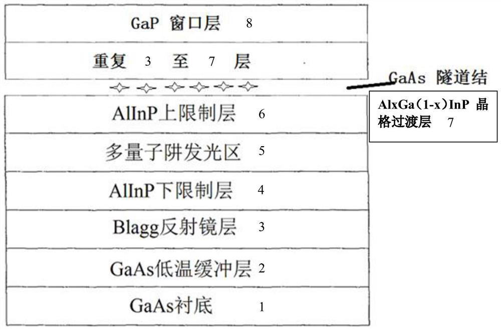
[0056] A GaAs-based multi-junction yellow-green LED, such as figure 1 As shown, from bottom to top, it includes GaAs substrate 1, GaAs low-temperature buffer layer 2, Blagg mirror layer 3, AlInP lower confinement layer 4, multiple quantum well light-emitting region 5, AlInP upper confinement layer 6, AlxGa(1-x)InP The lattice transition layer 7 and the tunnel junction of GaAs material, the Blagg reflector layer 3 to the AlxGa(1-x)InP lattice transition layer 7 are grown repeatedly, and finally the GaP window layer 8 is grown.

Embodiment 2

[0058] A GaAs-based multi-junction yellow-green LED, the structure of which is shown in Example 1, the difference is that the tunnel junction of the GaAs material is formed by a GaAs-doped P-type layer, a GaAs intrinsic layer and a GaAs-doped N-type layer.

Embodiment 3

[0060] A method for preparing a GaAs-based multi-junction yellow-green LED, comprising the steps of:

[0061] 1) GaAs substrate 1 is placed in the MOCVD equipment growth chamber, H 2 The environment is heated to 750±20°C and baked for 40 minutes, and the AsH 3 , remove water and oxygen on the surface of the GaAs substrate 1 to complete the surface heat treatment, and prepare for step 2);

[0062] 2) Slowly lower the temperature to 700±20°C, the cooling time is 80 seconds, and feed TMGa and AsH 3 , growing a GaAs low-temperature buffer layer 2 with a thickness of 0.5um on the GaAs substrate;

[0063] 3) Keep the temperature at 700±20°C, and continue to feed TMGa, TMAl and AsH 3 , growing a Bragg reflector layer 3 on the GaAs low-temperature buffer layer 2 grown in step 2), where the Bragg reflector layer 3 is AlGaAs;

[0064] 4) The temperature is lowered to 650±20°C, and an n-type AlInP lower confinement layer 4 is grown on the Bragg mirror layer 3 grown in step 3);

[00...


PUM

PropertyMeasurementUnit
Thicknessaaaaaaaaaa
Thicknessaaaaaaaaaa

Abstract

The invention relates to a GaAs-based multi-junction yellow-green light LED and a preparation method thereof, and belongs to the field of photoelectrons. The LED comprises a GaAs substrate, a GaAs low-temperature buffer layer, a Blagg reflector layer, an AlInP lower limiting layer, a multi-quantum well light-emitting region, an AlInP upper limiting layer, an AlxGa1-xInP lattice transition layer, atunnel junction of a GaAs material and a GaP window layer from bottom to top, wherein the tunnel junction of the GaAs material is formed by a GaAs doped P-type layer, a GaAs intrinsic layer and a GaAs doped N-type layer. According to the invention, after the AlInP upper limiting layer is grown, the tunnel junction of the GaAs material with high conductivity and lattice matching grows, and then the LED material with a conventional structure grows, so that the effect of luminous efficiency superposition is achieved on the premise of not increasing voltage, the cost of the device can be reduced,and the quantum efficiency can be greatly improved.

Description

technical field [0001] The invention relates to a GaAs-based multi-junction yellow-green LED and a preparation method thereof, belonging to the field of optoelectronic technology. Background technique [0002] LED itself has the advantages of small size, light weight, low heat generation, low power consumption, long life, good monochromaticity, fast response, environmental protection, and good shock resistance, so it is widely used in various fields. With the continuous advancement of technology and the change of people's life philosophy, quaternary AlGaInP yellow-green light-emitting diodes are widely used in various fields such as signal indication, traffic indication, automotive lighting, and special lighting. As the wavelength of quaternary AlGaInP materials shortens, the Al composition of the active layer increases continuously, and the combination of Al atoms with oxygen or carbon atoms leads to serious lattice defects in the material, and the luminous efficiency decre...

Claims


Application Information

Patent Timeline
IPC IPC(8): H01L33/06H01L33/08H01L33/10H01L33/32H01L33/00C30B25/18
CPCC30B25/183H01L33/0075H01L33/06H01L33/08H01L33/10H01L33/325
Inventor 徐晓强张兆喜吴向龙闫宝华王成新
Owner Shandong Huaguang Optoelectronics Co. Ltd.
Why Eureka
Try Eureka