
Gallium nitride growth method based on tin disulfide and magnetron sputtering aluminium nitride

A technology of tin disulfide and magnetron sputtering, which is applied in the field of electronics, can solve problems such as mismatch, large lattice, and difficulty in effectively alleviating substrate lattice mismatch, and achieve the effect of quality improvement

Active Publication Date: 2016-09-28
XIDIAN UNIV
View PDF5 Cites 5 Cited by
  • Summary
  • Abstract
  • Description
  • Claims
  • Application Information

AI Technical Summary

Problems solved by technology

However, the matching of silicon substrate and gallium nitride has the following problems: (1) has a large lattice mismatch; (2) has a large thermal expansion coefficient mismatch
However, the disadvantages of this method are: 1. The physical vapor deposition method requires a growth temperature of 1500°C, which is higher than the melting point of some substrates such as silicon, so it cannot be realized on substrates such as silicon.
2. The thickness of graphene is very thin, it is difficult to effectively alleviate the lattice mismatch between the substrate and gallium nitride, which greatly limits the selection range of substrates
However, the shortcomings of this method are: 1. Graphene is easy to decompose at high temperature to produce a large amount of C impurities, and the direct growth of GaN will make the impurities diffuse into the material and affect the material quality of GaN
2. The thickness of graphene is very thin, it is difficult to effectively alleviate the lattice mismatch between the substrate and gallium nitride, which greatly limits the selection range of substrates

Method used


Image

  • Gallium nitride growth method based on tin disulfide and magnetron sputtering aluminium nitride
  • Gallium nitride growth method based on tin disulfide and magnetron sputtering aluminium nitride

Examples


Embodiment 1

[0052] Embodiment 1: Ga-surface gallium nitride film based on tin disulfide and magnetron sputtering aluminum nitride.

[0053] Step 1. Prepare a tin disulfide transition layer.

[0054] First wash the four quartz ampoules A, B, C, and D with 10% hydrofluoric acid and then dry them thoroughly. Put the tin particles into the A quartz ampoule. The purity of the tin particles is 99.9%, and the amount of the substance is 4.08 mg. mol; the sulfur crystals are placed in the B quartz ampoule, the purity of the sulfur crystals is 99.9%, and the amount of the substance is 8.15 mmol; the iodine particles are placed in the C quartz ampoule, the purity of the iodine particles is 99.9%, and the mass is 2.0 per unit volume ~3.0 mg; four quartz ampoules A, B, C, D were then sealed. Put the three quartz ampoules A, B, and C into the front section of the two-stage quartz reaction furnace, put the D quartz ampoule into the back section of the two-stage quartz reaction furnace and open the four...

Embodiment 2

[0066] Embodiment 2: N-face gallium nitride film based on tin disulfide and magnetron sputtering aluminum nitride.

[0067] Step A. Preparation of tin disulfide transition layer:

[0068] First wash the four quartz ampoules A, B, C, and D with 10% hydrofluoric acid and then dry them thoroughly. Put the tin particles into the A quartz ampoule. The purity of the tin particles is 99.9%, and the amount of the substance is 4.08 mg. mol; the sulfur crystals are placed in the B quartz ampoule, the purity of the sulfur crystals is 99.9%, and the amount of the substance is 8.15 mmol; the iodine particles are placed in the C quartz ampoule, the purity of the iodine particles is 99.9%, and the mass is 2.0 per unit volume ~3.0 mg; four quartz ampoules A, B, C, D were then sealed. Put the three quartz ampoules A, B, and C into the front section of the two-stage quartz reaction furnace, put the D quartz ampoule into the back section of the two-stage quartz reaction furnace and open the fou...


PUM

PropertyMeasurementUnit
thicknessaaaaaaaaaa
thicknessaaaaaaaaaa
thicknessaaaaaaaaaa

Abstract

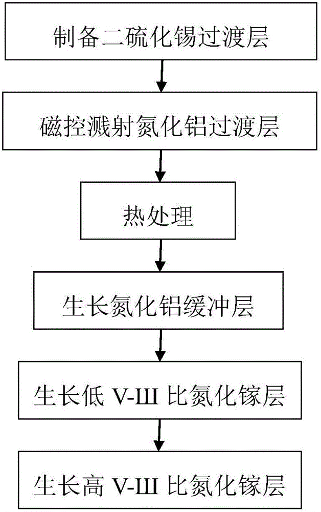
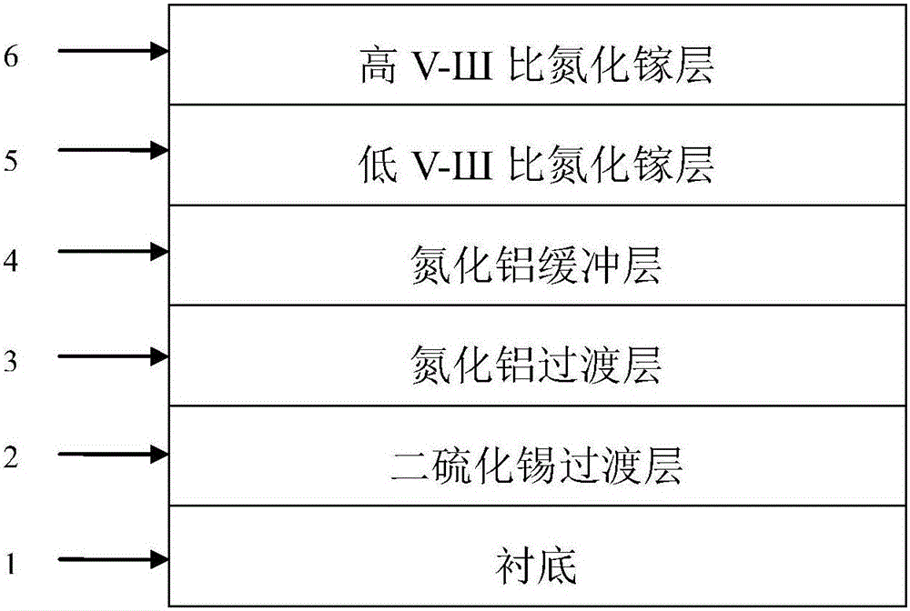
The invention discloses a gallium nitride growth method based on tin disulfide and magnetron sputtering aluminium nitride, aiming to improve the quality of gallium nitride materials. The method includes the growth steps of (1) tin disulfide transition layer preparation, (2) aluminium nitride transition layer magnetron sputtering, (3) heat treatment, (4) aluminium nitride buffer layer growth, (5) low V-III gallium nitride layer growth, and (6) high V-III gallium nitride layer growth. The gallium nitride film is advantageous in that through the combination with the tin disulfide and aluminium nitride subjected to magnetron sputtering, the material quality is good, applicable substrate range is large, and a high-performance nitride-based device can be manufactured.

Description

technical field [0001] The invention belongs to the field of electronic technology, and further relates to a gallium nitride growth method based on tin disulfide and magnetron sputtering aluminum nitride in the field of microelectronic technology. The invention can be used for making gallium nitride thin films and devices thereof. Background technique [0002] The third-generation semiconductors represented by gallium nitride have the advantages of large band gap, high breakdown field strength, high thermal conductivity, corrosion resistance and radiation resistance, and are widely used in optoelectronic devices and electronic devices. Recent progress in the growth of GaN-based materials on silicon substrates and their device applications has attracted great attention. However, the following problems exist in the matching of silicon substrate and gallium nitride: (1) large lattice mismatch; (2) large thermal expansion coefficient mismatch. These will lead to high defect de...

Claims


Application Information

Patent Timeline
Patent Type & Authority Applications(China)
IPC IPC(8): H01L21/02C23C14/35C23C14/06C23C16/34C23C28/04
CPCC23C14/0036C23C14/0617C23C14/35C23C16/303C23C28/04H01L21/02485H01L21/0254H01L21/0262
Inventor 张进成陈智斌庞凯吕佳骐朱家铎许晟瑞林志宇宁静张金风郝跃
Owner XIDIAN UNIV
Learn More