Growing method of ultraviolet LED active area multiple quantum well

A technology of multiple quantum wells and growth methods, which is applied in the field of growth of multiple quantum wells in the active area of ​​ultraviolet LEDs, can solve the problems of reducing the luminous efficiency of quantum wells, and achieves optimal concentration distribution, increased current injection efficiency, and reduced stress. Effect

Active Publication Date: 2016-09-28
宁波安芯美半导体有限公司
View PDF4 Cites 11 Cited by
  • Summary
  • Abstract
  • Description
  • Claims
  • Application Information

AI Technical Summary

Problems solved by technology

[0005] The technical problem to be solved by the present invention is to provide a method for growing multi-quantum wells in the active region of an ultraviolet LED, aiming at the problems caused by the strong polarized e...

Method used


Image

  • Growing method of ultraviolet LED active area multiple quantum well
  • Growing method of ultraviolet LED active area multiple quantum well

Examples


Embodiment 1

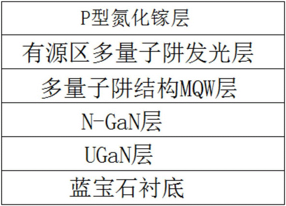
[0019] A method for growing multi-quantum wells in the active region of an ultraviolet LED. The epitaxial structure of the LED chip is in the order from bottom to top: sapphire substrate, UGaN layer, N-GaN layer, multi-quantum well structure MQW layer, active A multi-quantum well light-emitting layer and a p-type gallium nitride layer, the growth method of which comprises the following steps:

[0020] Step 1: On the sapphire substrate, adjust the temperature to 1000-1200°C, pass through TMGa, grow a UGaN layer with a thickness of 0.5-2.5um, the growth pressure is between 100-500Torr, V / III molar ratio Between 300-2500;

[0021] Step 2, after the growth of the UGaN layer is completed, grow a layer of N-GaN layer with a stable doping concentration, the thickness is 1.5-4.5um, the growth temperature is between 1000-1200°C, and the pressure is between 100-600Torr, V / Ⅲ molar ratio between 50-2000;

[0022] Step 3, after the growth of the N-GaN layer is completed, grow the multi-...

Embodiment 2

[0027] A method for growing multiple quantum wells in an active region of an ultraviolet LED, the growth method comprising the following steps:

[0028] Step 1: On the sapphire substrate, adjust the temperature to 1100°C, inject TMGa, and grow a UGaN layer with a thickness of 1.5um, the growth pressure is 300 Torr, and the V / III molar ratio is 500;

[0029] Step 2, after the growth of the UGaN layer is completed, a layer of N-GaN layer with a stable doping concentration is grown, the thickness is 2.5um, the growth temperature is 1100°C, the pressure is 300Torr, and the V / III molar ratio is 500;

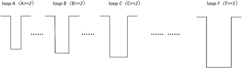
[0030]Step 3, after the growth of the N-GaN layer is completed, grow the multi-quantum well structure MQW layer, the growth temperature is 800 ° C, the growth pressure is 300 Torr, the V / III molar ratio is 2000, and the multi-quantum well structure MQW layer is composed of 1 -20 layers In x Ga 1-X It consists of N / GaN multiple quantum wells, the thickness of the multiple quantum wel...


PUM

PropertyMeasurementUnit
Thicknessaaaaaaaaaa
Thicknessaaaaaaaaaa
Thicknessaaaaaaaaaa

Abstract

The invention provides a growing method of an ultraviolet LED active area multiple quantum well. The growing method is characterized in that step1, a UGaN layer is grown on a sapphire substrate; step2, after the growing of the UGaN layer is ended, an N-GaN layer having stable doping concentration is grown; step 3, after the growing of the N-GaN layer is ended, a multiple quantum well structure MQW layer is grown; step 4, after the growing of the multiple quantum well structure MQW layer is ended, an active area multiple quantum well light-emitting layer is grown; step 5, after the growing of the active area multiple quantum well light-emitting layer is ended, a P-type gallium nitride layer taking N2 as a carrier gas is grown; step 6, after the growing of the P-type gallium nitride layer is ended, an LED epitaxial structure is acquired by adopting annealing treatment. By adopting the production technology provided by the invention, electron concentration distribution is optimized, and electron leakage is suppressed; stress generated during a multiple quantum well growing process is reduced, and quantum confinement stark effect (QCSE) is reduced; current injection efficiency is increased, and multiple quantum well light-emitting efficiency is improved.

Description

technical field [0001] The invention relates to the technical field of semiconductor devices, in particular to a method for growing multiple quantum wells in an active region of an ultraviolet LED. Background technique [0002] Ultraviolet Light-Emitting Diodes based on III-nitride wide bandgap semiconductor materials have broad applications in the fields of sterilization, polymer curing, special lighting, phototherapy, and biochemical detection. prospect. [0003] With the continuous development of LEDs, GaN-based high-brightness LEDs have been commercialized on a large scale, and have shown strong market potential in fields such as landscape lighting, backlight applications, and optical communications. At the same time, the development of white LED solid-state lighting is in full swing, which is triggering the third lighting revolution. With the gradual maturity of the field of visible light, people gradually shift the focus of research to ultraviolet LEDs with shorter w...

Claims


Application Information

Patent Timeline
IPC IPC(8): H01L33/00H01L33/06H01L33/12H01L33/14H01L33/32
CPCH01L33/007H01L33/06H01L33/12H01L33/14H01L33/32
Inventor 郭丽彬程斌唐军潘尧波
Owner 宁波安芯美半导体有限公司
Why Eureka
Try Eureka