Low-temperature low-pressure growth method and Raman spectrum characterization method of posphorus-doped N type germanium nano wire

A technology of germanium nanowires and Raman spectroscopy, which is applied to the low-temperature and low-pressure growth method of N-type germanium nanowires and the field of Raman spectroscopy characterization, and can solve problems that need to be further explored

Inactive Publication Date: 2016-10-05
WUHAN UNIV OF TECH
View PDF3 Cites 7 Cited by
  • Summary
  • Abstract
  • Description
  • Claims
  • Application Information

AI Technical Summary

Problems solved by technology

However, there is no simple and effective synthesis method that can obtain high-density and large-area doped germanium nanowire arrays at low temperature and low pressure.
[0003] Doping can change the Fermi level of the material and provide additional atoms, so that the electrical properties of the material after doping can be improved. However, how to characterize the doped nanowires simply and effectively remains to be further explored

Method used


Image

  • Low-temperature low-pressure growth method and Raman spectrum characterization method of posphorus-doped N type germanium nano wire
  • Low-temperature low-pressure growth method and Raman spectrum characterization method of posphorus-doped N type germanium nano wire
  • Low-temperature low-pressure growth method and Raman spectrum characterization method of posphorus-doped N type germanium nano wire

Examples


Embodiment 1

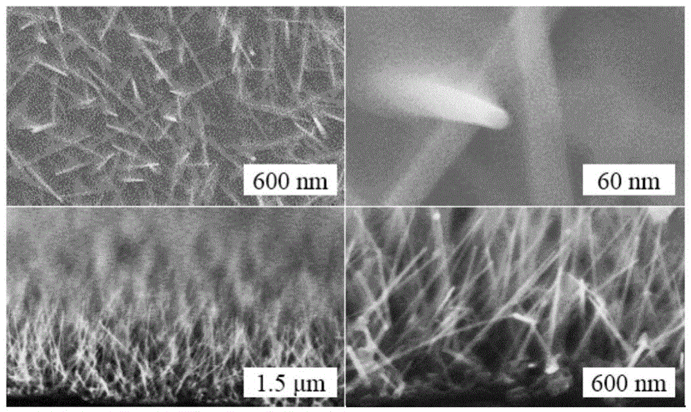
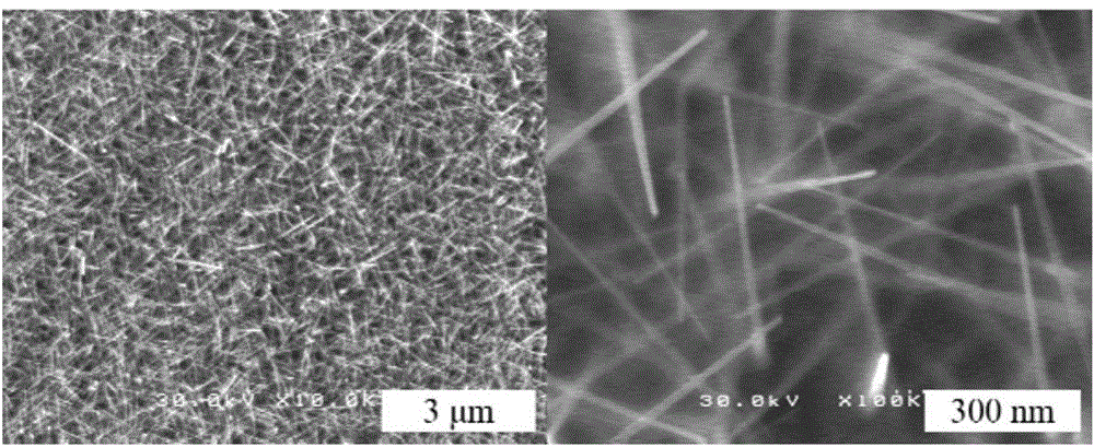
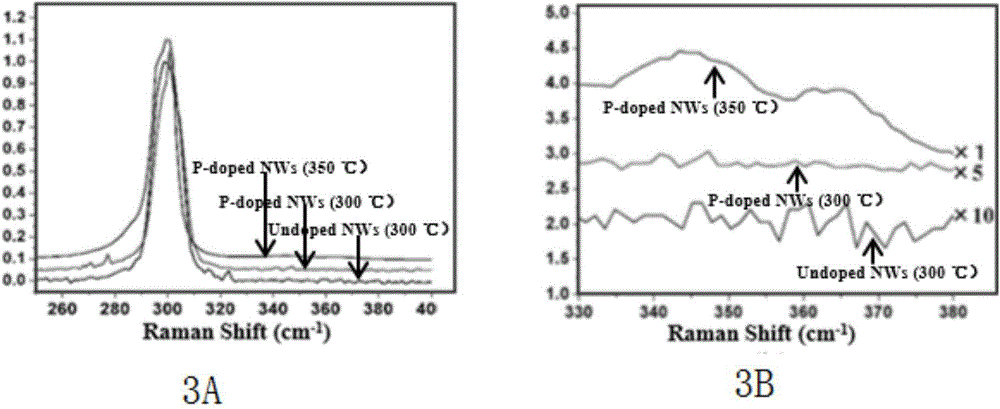
[0027] Example 1, see Figure 1 to Figure 3 Shown:

[0028] The invention provides a low-temperature and low-pressure growth method and a Raman spectrum characterization method of phosphorus-doped N-type germanium nanowires, which specifically include the following steps:

[0029] (1) Clean the silicon substrate with deionized water, the parameters of the silicon substrate are: impedance 0.2Ω·cm -1 , no oxide layer, double-sided polishing, (111) crystal plane, N-type;

[0030] (2) Clean the silicon substrate with ethanol, and then use deionized water to clean the silicon substrate;

[0031] (3) Clean the silicon substrate with a mixture of sulfuric acid and hydrogen peroxide, and then use deionized water to clean the silicon substrate;

[0032] (4) Treating the silicon substrate with 5% to 10% hydrofluoric acid solution to obtain a hydrogenated surface;

[0033] (5) Place the cleaned silicon substrate in an electron beam evaporator for evaporation of gold catalyst, and eve...

Embodiment 2

[0040] The invention provides a low-temperature and low-pressure growth method and a Raman spectrum characterization method of phosphorus-doped N-type germanium nanowires, which specifically include the following steps:

[0041] (1) Clean the silicon substrate with deionized water, the parameters of the silicon substrate are: impedance 0.2Ω·cm -1 , no oxide layer, double-sided polishing, (111) crystal plane, N-type;

[0042] (2) Clean the silicon substrate with ethanol, and then use deionized water to clean the silicon substrate;

[0043] (3) Clean the silicon substrate with a mixture of sulfuric acid and hydrogen peroxide, and then use deionized water to clean the silicon substrate;

[0044] (4) Place the cleaned silicon substrate in an electron beam evaporating device for evaporation of gold catalyst, and evenly plate gold nanoparticles on the silicon substrate to obtain a gold-plated silicon substrate. The evaporation current is 45mA. The plating rate is 0.1A / s, and the thi...

Embodiment 3

[0048] The invention provides a low-temperature and low-pressure growth method and a Raman spectrum characterization method of phosphorus-doped N-type germanium nanowires, which specifically include the following steps:

[0049] (1) Clean the silicon substrate with deionized water, the parameters of the silicon substrate are: impedance 0.2Ω·cm -1 , no oxide layer, single-sided polishing, (100) crystal plane, P type;

[0050] (2) Clean the silicon substrate with ethanol, and then use deionized water to clean the silicon substrate;

[0051] (3) Clean the silicon substrate with a mixture of sulfuric acid and hydrogen peroxide, and then use deionized water to clean the silicon substrate;

[0052] (4) Treating the silicon substrate with 5% to 10% hydrofluoric acid solution to obtain a hydrogenated surface;

[0053] (5) Place the cleaned silicon substrate in an electron beam evaporator for evaporation of gold catalyst, and evenly plate gold nanoparticles on the silicon substrate t...


PUM

PropertyMeasurementUnit
thicknessaaaaaaaaaa

Abstract

The invention provides a low-temperature low-pressure growth method and Raman spectrum characterization method of a posphorus-doped N type germanium nano wire. With GeH4 / H2 as the precursor of germanium nano wire growth, with PH3 / Ar as a doping source gas, under the catalysis of gold nanoparticles, by using low pressure chemical vapor deposition (LPCVD), a large-area ordered high-density posphorus-doped N type germanium nano wire is prepared on the silicon substrate under low temperature, and the gold nanoparticles are obtained through electron beam evaporation. The posphorus-doped N type germanium nano wire is characterized through a Raman spectrum. According to the invention, the related technology of the semiconductor field and the synthesis method of micro nano structures, a large-density large-area germanium nano wire array can be obtained in a low-temperature low-pressure condition, the process is simple, and the posphorus-doped germanium nano wire is effectively characterized by using the Raman spectrum.

Description

technical field [0001] The invention relates to the intersecting fields of nanomaterials, microprocessing technology and micro-nano devices, in particular to a low-temperature and low-pressure growth method and a Raman spectrum characterization method of phosphorous-doped N-type germanium nanowires. Background technique [0002] Compared with traditional materials, one-dimensional semiconductor nanowires have many unique properties, such as low-dimensional scale, quantum confinement effect, surface activity and energy band separation, etc., making them useful as functional micro-nano systems in the fields of electricity and optoelectronics. very attractive structural unit. Germanium nanowires, due to their small effective mass of electrons and holes, have high carrier mobility, and thus become ideal channel materials in semiconductor devices. In addition, as the fourth main group element, germanium (Ge) has many properties similar to silicon (Si), which makes germanium, lik...

Claims


Application Information

Patent Timeline
Patent Type & Authority Applications(China)
IPC IPC(8): H01L21/205
Inventor 何亮麦立强熊彪杨枭郝志猛罗雯
Owner WUHAN UNIV OF TECH
Why Eureka
Try Eureka