Organic and inorganic hybrid bismuth and iodine anionic cluster-based semiconductor material

A semiconductor and anion technology, applied in inorganic chemistry, organic chemistry, bismuth compounds, etc., to achieve the effects of good thermal stability, low production cost, and cheap purification

Inactive Publication Date: 2016-10-12
CHINA JILIANG UNIV
View PDF4 Cites 10 Cited by
  • Summary
  • Abstract
  • Description
  • Claims
  • Application Information

AI Technical Summary

Problems solved by technology

However, for today's technical application requirements, the available semiconductor materials are

Method used


Image

  • Organic and inorganic hybrid bismuth and iodine anionic cluster-based semiconductor material
  • Organic and inorganic hybrid bismuth and iodine anionic cluster-based semiconductor material
  • Organic and inorganic hybrid bismuth and iodine anionic cluster-based semiconductor material

Examples


Example Embodiment

[0026] Example 1

[0027] A large number of organic-inorganic hybrid bismuth iodine anion cluster-based semiconductor materials (MV) 2 (Bi 4 I 16 ) Preparation of crystal samples: Weigh 0.603g (1mmol) of bismuth iodide and dissolve it in 40ml of acetone to obtain a clear solution A, and weigh 0.222g (0.5mmol) of methylviologen iodide and dissolve it in 8ml of water to obtain a clear solution. Solution B; Then, the above solution B was added to solution A, and it immediately formed turbidity. After the addition was completed, the reaction was stirred and reacted for half an hour to form a large amount of crystal products. The crystals were separated by filtration, washed twice with water and ethanol, and dried in vacuum. A large number of deep red crystals are the target products of the hybrid material, and the yield exceeds 80%.

Example Embodiment

[0028] Example 2

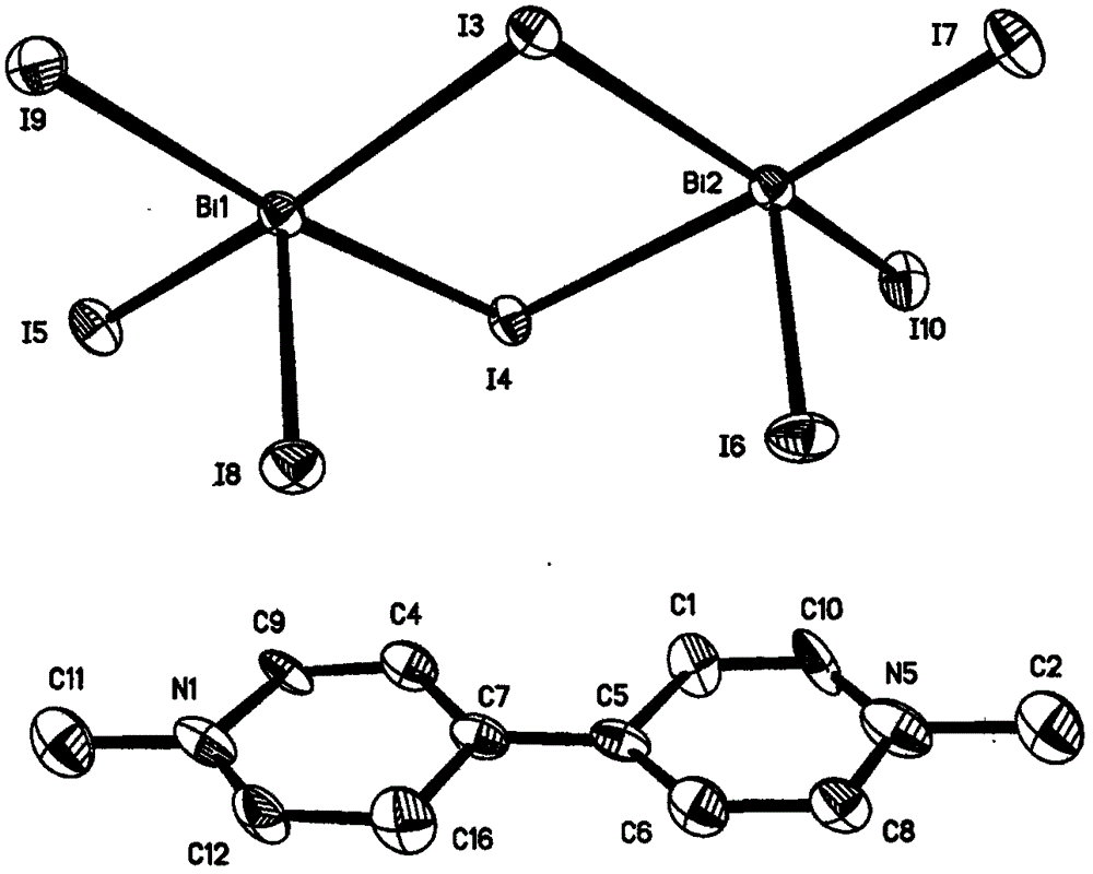
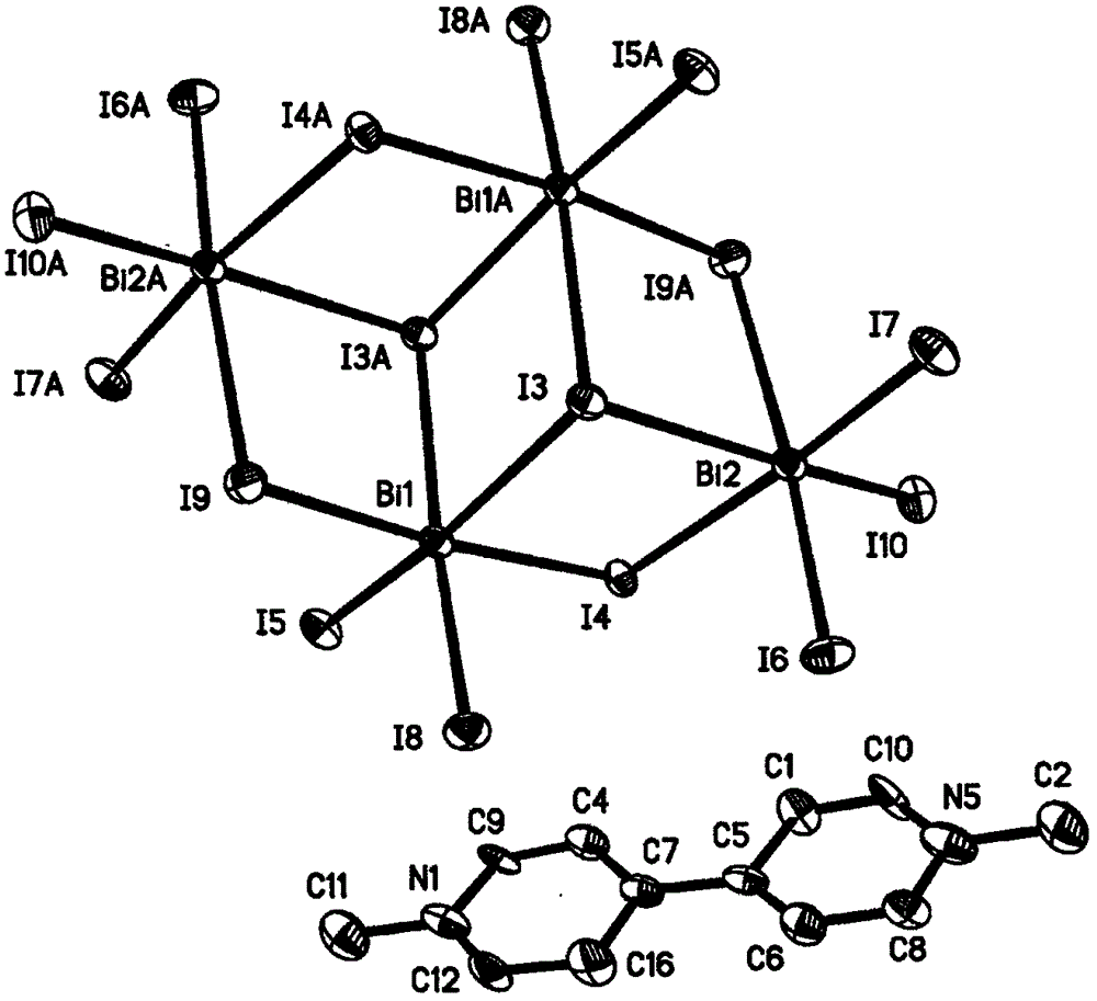
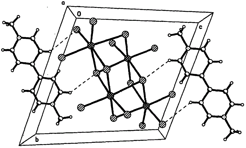
[0029] Synthesis of organic-inorganic hybrid bismuth iodine anion cluster-based semiconductor material (MV) 2 (Bi 4 I 16 ) Single crystal: Weigh 60mg (0.1mmol) of bismuth iodide dissolved in 5ml of acetone to obtain a clear solution A, weigh 22mg (0.05mmol) of methylviologen iodide dissolved in 5ml of water to obtain a clear solution B ; Then, first put solution B in a test tube, and then slowly add solution A to the test tube to make it on the upper layer of solution B, seal the test tube and let it stand, a few days later, a large number of dark red block crystals precipitated. A dark red block crystal with a size of 0.18mm*0.16mm*0.10mm is selected for X-ray single crystal structure test. The structure diagram of the crystallographic independent unit of this compound is attached figure 1 , The structure diagram of its bismuth iodide anion cluster and the corresponding counter cation methyl viologen is attached figure 2 , Its unit cell stacked structure diag...


PUM


Abstract

The invention discloses an organic and inorganic hybrid bismuth and iodine anionic cluster-based semiconductor material and a preparation method thereof. The molecular structural formula of the organic and inorganic hybrid semiconductor material is (MV)2(Bi4I16), MV in the formula is organic cationic methyl viologen with two unit positive charges, and the (Bi4I16) anion in the material is a four-nuclear cluster structural anion composed of trivalent bismuth ions and iodide ions. Through a coordination reaction between the bismuth iodide and a solution of methyl viologen iodide, the organic and inorganic hybrid semiconductor material which is good in semiconductor performance and thermal stability is conveniently prepared with low price, the organic and inorganic hybrid semiconductor material is moderate in energy gap and good in thermal stability and can be applied to the technical field of optoelectronic materials.

Description

technical field [0001] The invention relates to the technical field of semiconductor materials, to the field of inorganic cluster materials and organic-inorganic hybrid materials, in particular to the field of iodide-based semiconductor materials. Background technique [0002] Electronic technology is one of the foundations of modern science and technology, and it is also a prominent feature of modern science and technology. At present, electronic technology has penetrated into all fields of the national economy, and the rise of the electronic industry has also brought about extensive and profound technological innovations in the national economy. What plays a major role in electronic technology is the heart of electronic equipment-components made of semiconductor materials. From this point of view, semiconductor materials are the foundation of the electronics industry, and it is also the most important raw material for the electronics industry. Looking back at history, fr...

Claims


Application Information

Patent Timeline
IPC IPC(8): C07D213/22C01G29/00
CPCC01G29/00C07D213/22
Inventor 柴文祥吴晓云宋莉朱秋梦郭冰秦来顺沈杭燕陈海潮舒康颖
Owner CHINA JILIANG UNIV
Why Eureka
Try Eureka