Device and method for preparing amorphous carbon and nitrogen thin films on surface of silicon

An amorphous carbon nitrogen and silicon surface technology, applied in ion implantation plating, coating, metal material coating process, etc., can solve the problems of effective control of content and distribution, system research, etc., and achieve chemical bond content and structure. control, uniform structure distribution, and strong process operability

Active Publication Date: 2016-10-12
BEIJING WUKE GUOHUA TECH CO LTD
View PDF5 Cites 8 Cited by
  • Summary
  • Abstract
  • Description
  • Claims
  • Application Information

AI Technical Summary

Problems solved by technology

However, in the existing reports, there is no effective control and systematic research on the content and distribution of phase composition and bond structure, and the interaction between different nitrogen source supply methods and the energy and density of carbon ions also needs to be further studied.

Method used


Image

  • Device and method for preparing amorphous carbon and nitrogen thin films on surface of silicon
  • Device and method for preparing amorphous carbon and nitrogen thin films on surface of silicon
  • Device and method for preparing amorphous carbon and nitrogen thin films on surface of silicon

Examples


Embodiment 1

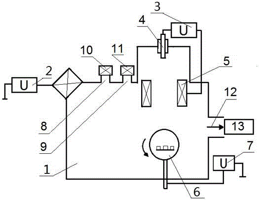
[0039] use figure 1 The shown device prepares atomized nitrogen-doped amorphous carbon-nitride film on the surface of silicon substrate.

[0040] A single crystal silicon substrate with a diameter of 20 mm and a thickness of 0.5 mm was tested, and the operation steps were as follows:

[0041] (1) Surface treatment of silicon substrate: Place the monocrystalline silicon wafer into acetone solution, ethanol solution and deionized water for 10 minutes to ultrasonically clean each to remove surface grease and other pollutants, then place the substrate in an oven to dry for use ;

[0042] (2) Fix the pretreated silicon substrate on such as figure 1 On the rotating sample stage in the vacuum chamber of the cathodic arc device shown, the high-purity graphite target is used as the cathode of the pulsed arc;

[0043] (3) Use a vacuum device to evacuate the vacuum chamber to make the vacuum degree reach 6×10 −4 Pa; argon gas is introduced into the vacuum chamber through the air i...

Embodiment 2

[0046] use figure 1 The shown device prepares an ionized nitrogen-doped amorphous carbon-nitride film on the surface of a silicon substrate.

[0047] A single crystal silicon substrate with a diameter of 20 mm and a thickness of 0.5 mm was tested, and the operation steps were as follows:

[0048] (1) Surface treatment of silicon substrate: Place the monocrystalline silicon wafer into acetone solution, ethanol solution and deionized water for 10 minutes to ultrasonically clean each to remove surface grease and other pollutants, then place the substrate in an oven to dry for use ;

[0049] (2) Fix the pretreated silicon substrate on such as figure 1 On the rotating sample stage in the vacuum chamber of the cathodic arc device shown, the high-purity graphite target is used as the cathode of the pulsed arc;

[0050] (3) Use a vacuum device to evacuate the vacuum chamber to make the vacuum degree reach 6×10 −4 Pa; argon gas is introduced into the vacuum chamber through the a...

Embodiment 3

[0055] use figure 1 The shown device prepares atomized nitrogen-doped amorphous carbon-nitride film on the surface of silicon substrate.

[0056] A single crystal silicon substrate with a diameter of 20 mm and a thickness of 0.5 mm was tested, and the operation steps were as follows:

[0057] (1) Surface treatment of silicon substrate: Place the monocrystalline silicon wafer into acetone solution, ethanol solution and deionized water for 10 minutes to ultrasonically clean each to remove surface grease and other pollutants, then place the substrate in an oven to dry for use ;

[0058] (2) Fix the pretreated silicon substrate on such as figure 1 On the rotating sample stage in the vacuum chamber of the cathodic arc device shown, the high-purity graphite target is installed on the pulsed cathodic arc power supply;

[0059] (3) Use a vacuum device to evacuate the vacuum chamber to make the vacuum degree reach 6×10 −4 Pa; argon gas is introduced into the vacuum chamber throu...


PUM

PropertyMeasurementUnit
thicknessaaaaaaaaaa

Abstract

The invention discloses a device and method for preparing amorphous carbon and nitrogen thin films on the surface of silicon. The device is a pulse cathode electric arc device assisted by an ion source. The preparation device includes the following steps that a silicon substrate which is chemically cleaned in advance is dried and placed on a rotating sample table; vacuumization is performed, argon gas is led into a vacuum chamber, and the surface of the silicon substrate is physically cleaned through an ion sputtering source; and high-purity graphite serves as a cathode target material of a pulse electric arc, the pulse discharging frequency is adjusted, nitrogen gas is led at the same time, the ion source is opened, and the atomization and ionization nitrogen-doped amorphous carbon and nitrogen thin films are prepared. By means of the device and method, the content of carbon/nitrogen atoms and carbon-nitrogen bonds/carbon-carbon bonds in the amorphous carbon and nitrogen thin films is adjustable, and the carbon and nitrogen bonding types and the graphite-like nitrogen/ pyridine-like nitrogen structures are controllable.

Description

Technical field [0001] The invention involves a device and method for preparing a non -crystal carbon nitrogen film on the silicon surface, which is a technical field of material surface modification. Background technique [0002] It is theoretically predicted by β-c 3 N 4 Since the stability of carbon nitrogen asia, the research of carbon nitride has aroused great interest in science and technology workers because β-C 3 N 4 The hardness of the structure may be close to or even more than diamonds, and the application of carbon nitrogen film in the fields of optics, electrical and machinery shows more excellent performance than the corresponding carbon film.Among them, the key to the successful application of these properties is to control the relative content of carbon and nitrogen atoms in the film and its key convergence structure (SP 2 -sP 2 , SP 3 -sP 3 And SP 2 -sP 3 ) Type and distribution.Although in the experiment, C 3 N 4 The seeking work of the crystal is still unsucces...

Claims


Application Information

Patent Timeline
Patent Type & Authority Applications(China)
IPC IPC(8): C23C14/06C23C14/32C23C14/02
CPCC23C14/0021C23C14/022C23C14/0658C23C14/325
Inventor 周兵刘竹波王志峰
Owner BEIJING WUKE GUOHUA TECH CO LTD
Why Eureka
Try Eureka