Manufacturing method for short wave UV LED chip having high reflection ohmic contact electrode

A technology of ohmic contact electrodes and LED chips, which is applied to circuits, electrical components, semiconductor devices, etc., can solve the problems of difficulty in light extraction, difficulty in improving crystal quality, and difficulty in doping and activation, achieving high reflectivity and improving light extraction efficiency. Effect

Inactive Publication Date: 2016-10-12
MINNAN NORMAL UNIV +1
View PDF5 Cites 6 Cited by
  • Summary
  • Abstract
  • Description
  • Claims
  • Application Information

AI Technical Summary

Problems solved by technology

[0007] The object of the present invention is to provide a short-wave ultraviolet LED chip manufacturing method with highly reflective ohmic contact electrodes, aiming to solve the problem of manufacturing 210-365nm ultraviolet LEDs, especially when the wavelength is shorter, the aluminum content in the material AlxGa1-xN is higher, and the crystal quality The more difficult it is to improve, the doping and activation of the P-type AlxGa1-xN layer is difficult, and the ultraviolet-reflecting metal is difficult to form an ohmic contact with the P-type GaN. The total internal reflection of the ultraviolet light in the chip in the AlxGa1-xN crystal makes it difficult to emit light. question

Method used


Image

  • Manufacturing method for short wave UV LED chip having high reflection ohmic contact electrode
  • Manufacturing method for short wave UV LED chip having high reflection ohmic contact electrode
  • Manufacturing method for short wave UV LED chip having high reflection ohmic contact electrode

Examples


Embodiment Construction

[0029] In order to make the objectives, technical solutions and advantages of the present invention clearer, the present invention will be further described in detail below in conjunction with embodiments. It should be understood that the specific embodiments described herein are only used to explain the present invention, but not to limit the present invention.

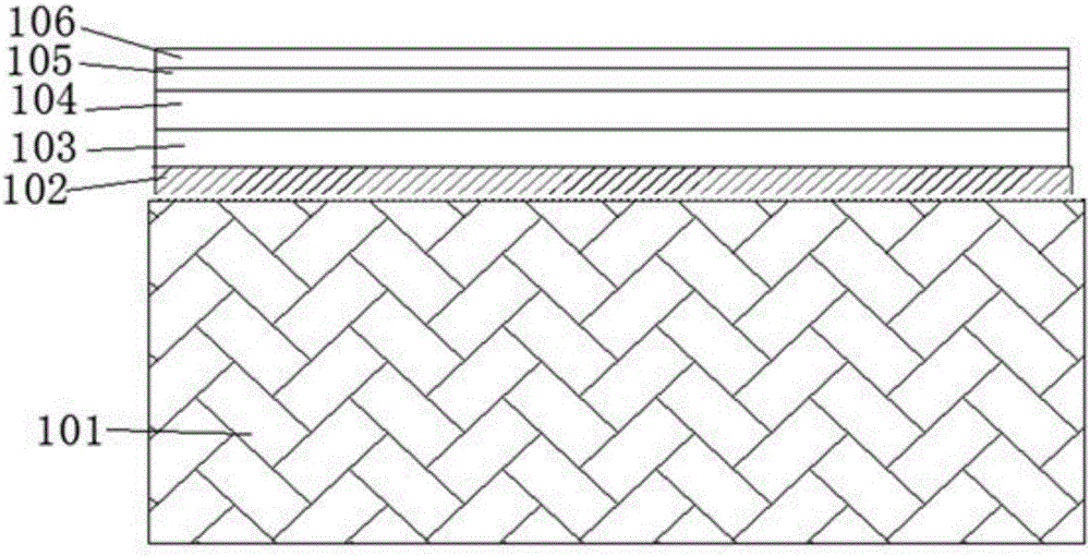
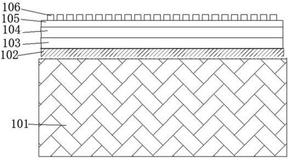
[0030] Such as figure 1 As shown, the present invention is realized in this way. The method for manufacturing a short-wave ultraviolet LED chip with highly reflective ohmic contact electrodes includes the following steps:

[0031] Step S101, growing Al with an ultraviolet quantum well structure on the substrate x Ga 1-x N semiconductor single crystal film, structure I is obtained;

[0032] Step S102, the semiconductor film is lithographically etched and etched to the P-type AlxGa1-xN layer, leaving a P-type GaN cylinder with a diameter of 0.3-5 microns and a thickness of less than 0.2 microns, P-GaN The column spacing is 0...


PUM


Abstract

The invention discloses a manufacturing method for a short wave UV LED chip having a high reflection ohmic contact electrode. According to the method, an AlxGa1-xN semiconductor monocrystalline film having an UV quantum well structure grows on a substrate, a structure I is acquired, and the x is greater than or equal to 0 and is smaller than or equal to 1; photoetching and etching of the semiconductor film are carried out, etching is carried out to an AlxGa1-xN layer, P-type GaN layer cylinders are acquired, P-type GaN cylinder intervals are in a range of 0.3-6 micrometer, a chip pattern is defined through photoetching of the semiconductor film, and penetration-through etching or non-penetration-through etching is carried out; a high reflection ohmic contact layer and a blocking layer are made, the chip is transferred onto a conductive substrate through a mode of bonding or electroplating or a mixed bonding and electroplating mode, an UV LED device is finally manufactured. Relatively good reflection ohmic contact is formed at P-type GaN and P-type AlxGa1-xN layers of the UV LED through employing Ni / Al, Pt / Al, Pd / Al and so on metal lamination layers having relatively high reflectivity for UV light, and ultraviolet light emitting efficiency is improved.

Description

Technical field [0001] The invention belongs to the field of semiconductor technology, and in particular relates to a method for manufacturing a short-wave ultraviolet LED chip with highly reflective ohmic contact electrodes. Background technique [0002] Ultraviolet (UV) light is divided into: UVA (ultraviolet rays with a wavelength of 315-400nm), UVB (ultraviolet rays with a wavelength of 280-315nm, and UVC (ultraviolet rays with a wavelength less than 280nm). The main uses of UVA and UVB include ultraviolet curing, document and Paper currency identification, medical treatment, printing, and air fresheners using photocatalysts, etc.; UVC is mainly used for sterilization, biochemical testing, high-density information storage, and military confidential communications. Because UV LEDs are energy-saving, environmentally friendly, lightweight, and spectral It has the advantages of purity, safety, and no mercury pollution, so it has gradually replaced the traditional ultraviolet ligh...

Claims


Application Information

Patent Timeline
Patent Type & Authority Applications(China)
IPC IPC(8): H01L33/04H01L33/32H01L33/00
CPCH01L33/0075H01L33/0093H01L33/04H01L33/32
Inventor 汤英文
Owner MINNAN NORMAL UNIV
Why Eureka
Try Eureka