High-contrast-grating coupled-cavity narrow-spectral-line-width surface-emitting laser

A high-contrast grating and emitting laser technology, applied in the field of optoelectronics, can solve problems such as restricting the application of VCSELs, and achieve the effects of simplifying fabrication difficulty, improving yield and reliability, and simplifying design and fabrication

Active Publication Date: 2016-10-26
BEIJING UNIV OF TECH
View PDF5 Cites 23 Cited by
  • Summary
  • Abstract
  • Description
  • Claims
  • Application Information

AI Technical Summary

Problems solved by technology

However, the spectral linewidth of the current fundamental transverse mode single-polarization VCSEL is 100MHz, which limits the application of VCSEL in microsystems such as atomic sensing. Research on the preparation of high-performance VCSEL devices to meet the application of new microsystems such as atomic clocks has become a research topic for people. The hot issue, the core of which is to prepare VCSEL devices with narrow spectral linewidth

Method used


Image

  • High-contrast-grating coupled-cavity narrow-spectral-line-width surface-emitting laser
  • High-contrast-grating coupled-cavity narrow-spectral-line-width surface-emitting laser

Examples


Embodiment Construction

[0018] The following is attached Figure 1-2 And embodiment the present invention is described in further detail.

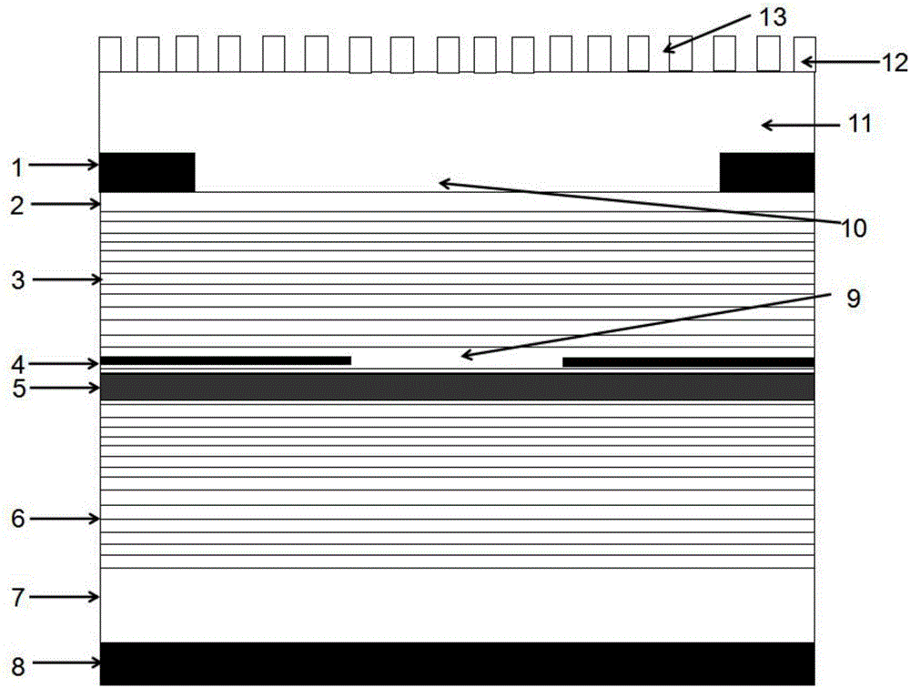
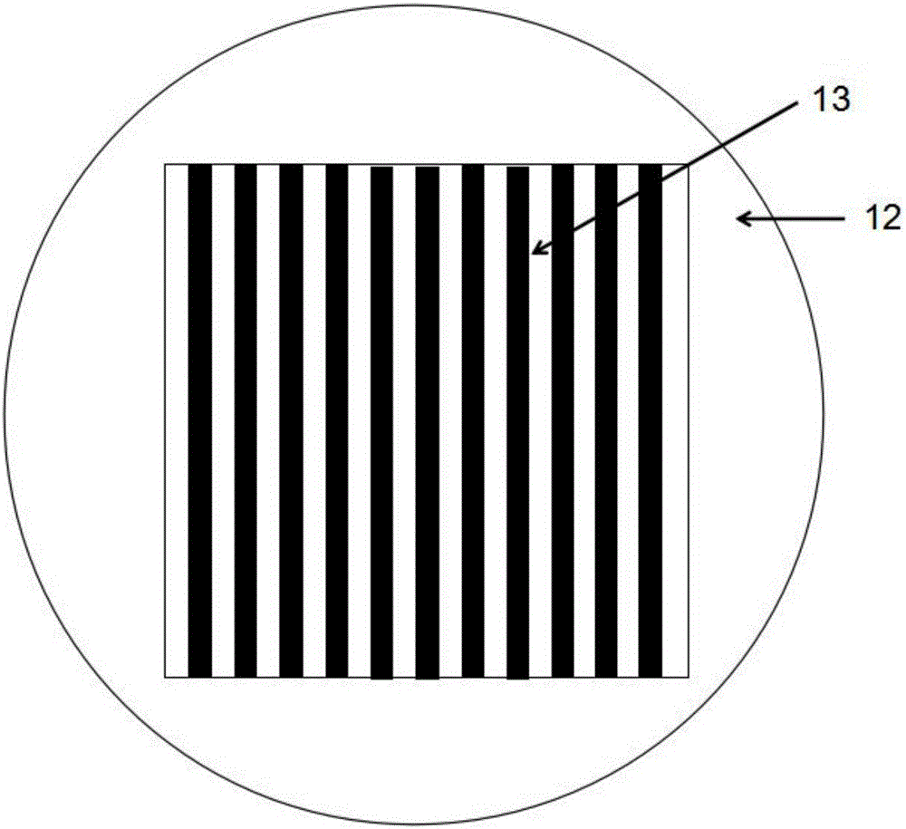
[0019] In order to achieve the above-mentioned purpose, the integrated high-contrast grating planar external cavity narrow-linewidth surface-emitting laser of the present invention adopts a brand-new physical idea, adopts epitaxial growth technology and semiconductor planar micro-nano processing technology, and carries out a brand-new design and production of the device . The device material is grown by MOCVD or MBE epitaxial growth technology, and the specific manufacturing process is as follows: grow lower DBR6, active region 5, Al 0.98 Ga 0.02Oxidation limiting layer of As high aluminum composition 4, upper distributed Bragg reflector (upper DBR) 3 with periodic alternate growth, P-type ohmic contact layer 2, upper metal electrode (P-type metal electrode) 1, N-type metal electrode 8 set At the bottom of the substrate 7, the oxidation hole 9 is set in the Al...


PUM


Abstract

The invention, which belongs to the technical field of the photoelectron, discloses a high-contrast-grating coupled-cavity narrow-spectral-line-width surface-emitting laser. A high-contrast grating having high reflectivity and large reflecting width is used as a reflector and is integrated to the top of a transverse-mode-based vertical-cavity surface-emitting laser; and on the basis of the high reflectivity of the high-contrast grating, emergent light of a device is fed back and photoinjection is carried out on the device, thereby obtaining a novel coupled-cavity integrated surface-emitting laser. Therefore, extension of an effective resonant cavity of the device is realized; and the spectral line width of the transverse-mode-based vertical-cavity surface-emitting laser is reduced to obtain a narrow-spectral-line-width surface-emitting laser. Because of utilization of the high-contrast-grating structure with support of the low refractive index, the integrated outer cavity preparation difficulty is reduced and the device processing process is simplified; the preparation process is a pure planar process, so that the yield and reliability of the device are improved effectively. The laser has advantages of large spectral line width adjusting range, obvious narrowing effect, and simple design and preparation process.

Description

technical field [0001] The invention belongs to the technical field of optoelectronics, and in particular relates to the design and manufacture of a novel integrated external cavity vertical cavity surface emitting semiconductor laser. Suitable for vertical cavity surface emitting semiconductor lasers with various wavelengths (650nm, 850nm, 852nm 980nm, 1064nm, 1310nm and 1550nm, etc.). Background technique [0002] Vertical-cavity surface-emitting lasers (Vertical-cavity surface-emitting lasers, VCSELs) are used in short-distance data transmission due to their low cost, low power consumption, easy packaging, high beam quality, and excellent high-speed modulation characteristics under low current conditions. , optical interconnection, optical storage and other aspects have a very good application. However, due to the disadvantages of multi-transverse-mode lasing and unstable polarization directions, ordinary VCSELs limit their applications in the fields of sensing and chip-...

Claims


Application Information

Patent Timeline
Patent Type & Authority Applications(China)
IPC IPC(8): H01S5/183
CPCH01S5/18386
Inventor 解意洋徐晨王秋华荀孟潘冠中董毅博安亚宁
Owner BEIJING UNIV OF TECH
Why Eureka
Try Eureka