

Method for introducing solid impurities into silicon material under room temperature environment
A silicon material and solid impurity technology, applied in semiconductor/solid-state device manufacturing, electrical components, circuits, etc., can solve problems that are difficult to be widely used in industrial production, high cost, and pollute the environment
- Summary
- Abstract
- Description
- Claims
- Application Information
AI Technical Summary
Problems solved by technology
Method used
Image

Examples
Embodiment 1
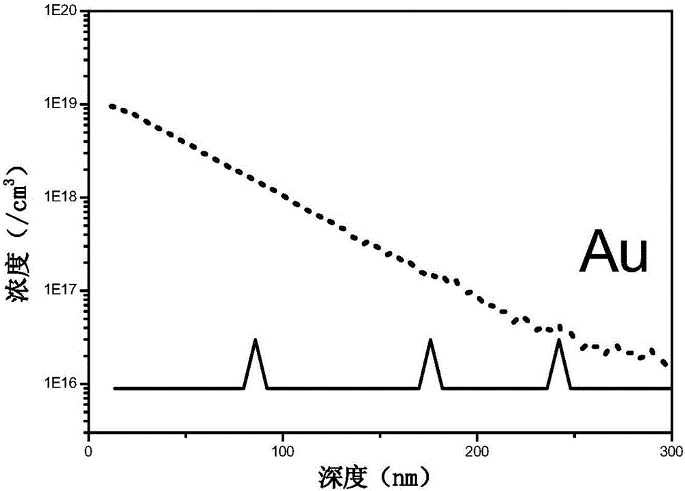
[0026] A P-type solar-grade Czochralski silicon single wafer is selected, polished on one side, with a resistivity of 1.9Ω·cm and a thickness of 625μm. First, silicon wafers were ultrasonically cleaned with acetone, ethanol, and deionized water for 10 min, and then immersed in 2% HF solution to remove the natural oxide layer on the silicon wafer surface. Then the gold foil is placed in the center of the bottom of the plasma reaction chamber, the silicon wafer faces the gold foil, and is placed in an area at a certain distance from the center of the bottom of the plasma reaction chamber. The working gas is helium, the flow rate is 22sccm, and the vacuum degree is about 5E-3Pa. The power of the excitation power supply is 750W, and the processing time is 2min. Finally, the SIMS method was used to obtain the distribution of Au impurity concentration with depth in the sample after plasma treatment. The results are as follows: figure 1 shown. After 750W plasma treatment, the high...
Embodiment 2
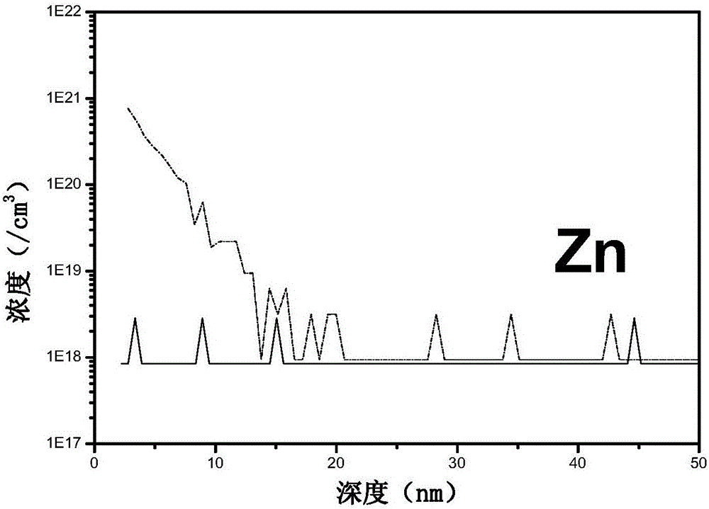
[0028] A P-type solar-grade Czochralski silicon single wafer is selected, polished on one side, with a resistivity of 1.9Ω·cm and a thickness of 625μm. First, silicon wafers were ultrasonically cleaned with acetone, ethanol, and deionized water for 10 min, and then immersed in 2% HF solution to remove the natural oxide layer on the silicon wafer surface. Next, the zinc ingot is placed in the center of the bottom of the plasma reaction chamber, and the silicon sheet faces the zinc ingot, and is placed in an area at a certain distance from the center of the bottom of the plasma reaction chamber. The working gas is helium, the flow rate is 22sccm, and the vacuum degree is about 5E-3Pa. The power of the excitation power supply is 750W, and the processing time is 2min. Finally, the SIMS method was used to obtain the distribution of Zn impurity concentration with depth in the sample after plasma treatment. The results are as follows: figure 2 shown. After 750W plasma treatment, ...
PUM
| Property | Measurement | Unit |
|---|---|---|
| Resistivity | aaaaa | aaaaa |
| Thickness | aaaaa | aaaaa |
Abstract
Description
Claims
Application Information