Preparation method of low temperature polysilicon film

A low-temperature polysilicon and polysilicon layer technology, applied in semiconductor/solid-state device manufacturing, electrical components, circuits, etc., can solve the problems affecting the electrical performance of the device, the offset of the flat-band voltage Vfb, and the reduction of the silicon channel current, so as to improve the current carrying capacity. effect of sub-migration speed, reduction of channel current loss, and reduction of heat loss

Active Publication Date: 2016-11-16
CHANGSHA HKC OPTOELECTRONICS CO LTD
View PDF4 Cites 6 Cited by
  • Summary
  • Abstract
  • Description
  • Claims
  • Application Information

AI Technical Summary

Problems solved by technology

[0011] In the prior art, since the film forming speed of the SiOx layer is Much faster than the film forming speed of amorphous silicon layer During the film formation of the SiOx layer, there will be more lattice defects, and at the same time, Si-H bonds or dangling bonds will be generated at the interface between the SiOx layer and the amorphous silicon layer, which will reduce the silicon channel current to a certain extent and cause flattening. The band voltage Vfb shifts, which affects the properties of the polysilicon layer, thereby affecting the electrical performance of the device
[0012] In view of the above-mentioned problems, in this field, it is hoped to seek an improved process for the formation of polysilicon. During the chemical vapor deposition of silicon oxide, it is divided into two steps, and the speed of the two-step chemical vapor deposition of silicon oxide is different, so that it can be Effectively solve the problem of high current in the silicon channel and the shift of the flat-band voltage Vfb, which affects the properties of polysilicon, and then affects the electrical performance of the device

Method used


Image

  • Preparation method of low temperature polysilicon film
  • Preparation method of low temperature polysilicon film
  • Preparation method of low temperature polysilicon film

Examples


Embodiment Construction

[0046] The following will clearly and completely describe the technical solutions in the embodiments of the present invention with reference to the accompanying drawings in the embodiments of the present invention. Obviously, the described embodiments are only some, not all, embodiments of the present invention. Based on the embodiments of the present invention, all other embodiments obtained by persons of ordinary skill in the art without making creative efforts belong to the protection scope of the present invention.

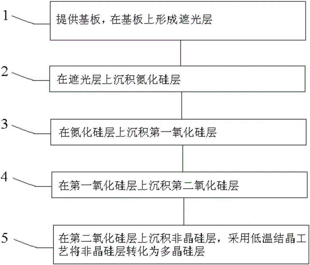
[0047] as per figure 1 The process shown in the preparation of low-temperature polysilicon thin film includes the following steps:

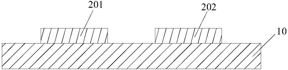
[0048] providing a substrate, and forming a light-shielding layer on the substrate;

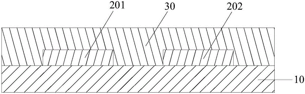
[0049] Depositing a silicon nitride layer on the light shielding layer;

[0050] depositing a first silicon oxide layer on the silicon nitride layer;

[0051] depositing a second silicon oxide layer on the first silicon oxide layer;

[0052]...


PUM


Abstract

The invention provides a preparation method of a low temperature polysilicon film. The method comprises a step of forming a light shield layer on a substrate, a step of depositing a silicon nitride layer on the light shield layer, a step of depositing a first silica layer with a first deposition speed and then depositing a second silica layer with a second deposition speed, and a step of depositing an amorphous silicon layer on the second silica layer such that the amorphous silicon layer is converted into a polysilicon layer, wherein the first deposition speed is larger than the second deposition speed. According to the method, the problem of influencing the quality of polysilicon and thus influencing the optical performance of a device by high silicon channel current and flat band voltage Vfb deviation can be solved.

Description

technical field [0001] The invention relates to the field of display technology, in particular to a method for preparing a low-temperature polysilicon thin film. Background technique [0002] Low temperature polysilicon (LTPS) thin film transistor liquid crystal display is different from the traditional amorphous silicon thin film transistor liquid crystal display, and it is developing rapidly. Its biggest advantage is ultra-thin, light weight, and low power consumption. , can provide more vivid colors and clearer images. [0003] Its electron mobility can reach 200cm 2 / V-sec or more can effectively reduce the area of ​​the thin film transistor device, thereby increasing the aperture ratio, and reducing the overall power consumption while increasing the brightness of the display. In addition, the higher electron mobility can integrate part of the driving circuit on the glass substrate, reducing the number of driving ICs, and can also greatly improve the reliability of the...

Claims


Application Information

Patent Timeline
Patent Type & Authority Applications(China)
IPC IPC(8): H01L21/02
CPCH01L21/02595
Inventor 王尧
Owner CHANGSHA HKC OPTOELECTRONICS CO LTD
Why Eureka
Try Eureka