Epitaxial wafer for inverted LED chip and fabrication method of epitaxial wafer

A technology of LED chips and epitaxial wafers, applied in electrical components, circuits, semiconductor devices, etc., can solve the problem that the current expansion ability affects the luminous efficiency and yield of the LED epitaxial structure, so as to enhance the current expansion ability, increase the injection efficiency, manufacture simple craftsmanship

Inactive Publication Date: 2016-11-16
YANGZHOU CHANGELIGHT
View PDF7 Cites 8 Cited by
  • Summary
  • Abstract
  • Description
  • Claims
  • Application Information

AI Technical Summary

Problems solved by technology

The brightness of the LED can be greatly improved by adopting the flip-chip structure. However, the current spreading ability of the n-s

Method used


Image

  • Epitaxial wafer for inverted LED chip and fabrication method of epitaxial wafer
  • Epitaxial wafer for inverted LED chip and fabrication method of epitaxial wafer
  • Epitaxial wafer for inverted LED chip and fabrication method of epitaxial wafer

Examples


Embodiment Construction

[0021] 1. Preparation process:

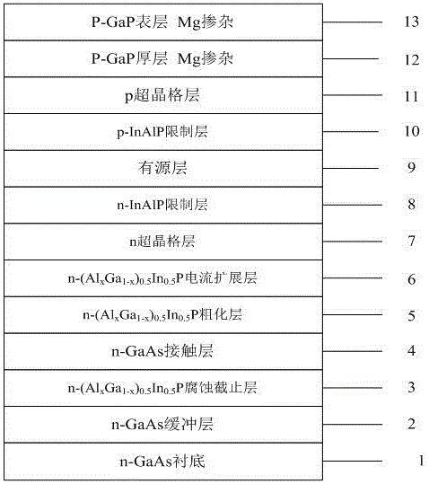
[0022] like figure 1 As shown, the n-GaAs buffer layer 2 is epitaxially grown from bottom to top on the n-GaAs substrate 1 by metal organic chemical vapor deposition (MOCVD), n-(Al x Ga 1-x ) 0.5 In 0.5 P etch stop layer 3, n-GaAs contact layer 4, n-(Al x Ga 1-x ) 0.5 In 0.5 P roughening layer 5, n-(Al x Ga 1-x ) 0.5 In 0.5 P current spreading layer 6, n-type superlattice layer 7, n-InAlP confinement layer 8, active layer 9, p-InAlP confinement layer 10, p-type superlattice layer 11, p-GaP window layer.

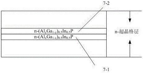
[0023] Wherein, n-type superlattice layer 7 is made of n-(Al x Ga 1-x ) 0.5 In 0.5 P potential well layer and n-(Al y Ga 1-y ) 0.5 In 0.5 The P potential barrier layers are periodically grown and formed, 0.42 h 6 as a source of doping. The thickness of the single periodic superlattice of the n-type superlattice layer is 5nm-20nm.

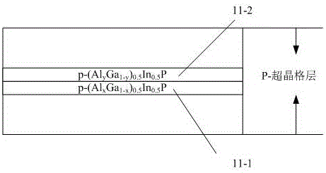
[0024] The p-type superlattice layer 11 is made of p-(Al x Ga 1-x ) 0.5 In 0.5 P potent...


PUM

PropertyMeasurementUnit
Total thicknessaaaaaaaaaa

Abstract

The invention relates to an epitaxial wafer for an inverted LED chip and a fabrication method of the epitaxial wafer, belongs to the technical field of epitaxy of a light emitting diode. An n-(Al<x>Ga<1-x>)<0.5>In<0.5>P potential well layer and an n-(Al<y>Ga<1-y>)<0.5>In<0.5>P barrier layer are periodically, alternatively and epitaxially grown during growth of an n-type superlattice, and a p-(Al<x>Ga<1-x>)<0.5>In<0.5>P potential well layer and a p-(Al<y>Ga<1-y>)<0.5>In<0.5>P barrier layer are periodically, alternatively and epitaxially grown during growth of a p-type superlattice. The fabrication process is simple and reasonable, the transverse motion of an electron in an n-(Al<x>Ga<1-x>)<0.5>In<0.5>P current extension layer can be effectively improved by the n-type superlattice, and the luminous efficiency of an AlGaInP epitaxial structure is further improved. With the product fabricated by the method, the luminous efficiency, the photoelectric property and the yield of an AlGaInP-based inverted LED epitaxial wafer can be effective enhanced.

Description

technical field [0001] The invention belongs to the technical field of epitaxial extension of light emitting diodes, in particular to a preparation technology for epitaxial wafers of flip-chip LED chips. Background technique [0002] In recent years, high-brightness quaternary AlGaInP light-emitting diodes have the characteristics of low power consumption, high luminous efficiency, long life, small size, and low cost, so they are widely used in lighting and optical fiber communication systems. Quaternary system (Al x Ga 1-x ) 0.5 In 0.5 The P material system can match the lattice of the GaAs substrate and with the change of the Al composition, the direct bandgap can change from 1.9cV to 2.3cv, and the wavelength can be from 560nm to 650nm, and then the emission from green to red can be realized. Based on the quaternary system (Al x Ga 1-x ) 0.5 In 0.5 There are many ways to improve the luminous efficiency of LEDs with P material system. Adopting the flip-chip struct...

Claims


Application Information

Patent Timeline
IPC IPC(8): H01L33/00H01L33/04H01L33/14H01L33/30
CPCH01L33/04H01L33/0062H01L33/14H01L33/30
Inventor 田海军林鸿亮赵宇石峰杨凯张双翔
Owner YANGZHOU CHANGELIGHT
Why Eureka
Try Eureka