
Tunnel field effect transistor with increased on state current

A technology of tunneling field effect and on-state current, which is applied in circuits, diodes, electrical components, etc., can solve the problems of high cost and incompatibility, and achieve the effect of low cost, large off-state current, and increased on-state current

Inactive Publication Date: 2016-12-07
UNIV OF ELECTRONICS SCI & TECH OF CHINA
View PDF4 Cites 2 Cited by
  • Summary
  • Abstract
  • Description
  • Claims
  • Application Information

AI Technical Summary

Problems solved by technology

The source region 1 material is GaAs 0.4 Sb 0.6 , the material of intrinsic region 2 and drain region 3 is In 0.65 Ga 0.35 As, at this time, the substrate generally requires a III-V compound semiconductor buffer layer, resulting in the incompatibility of this type of device fabrication with the traditional CMOS process line, and the cost is very high

Method used


Image

  • Tunnel field effect transistor with increased on state current
  • Tunnel field effect transistor with increased on state current
  • Tunnel field effect transistor with increased on state current

Examples


Embodiment 1

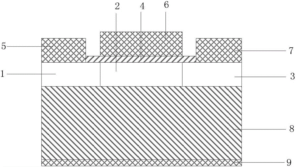
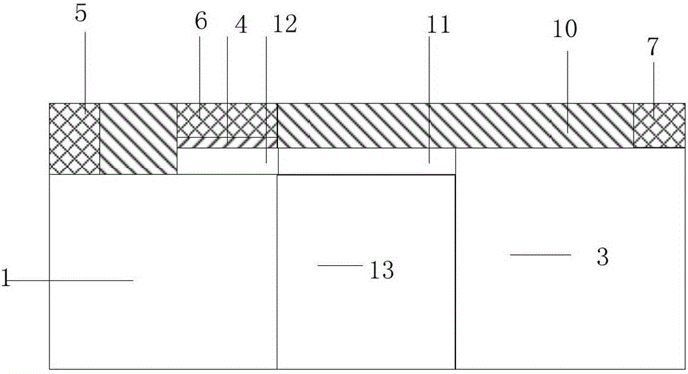
[0030] This example is for image 3 The structure of the TFET device with increased on-state current is shown, taking the N-type TFET fabricated on Si material as an example, and the insulating low-K dielectric is made of SiO 2 , Si, and vacuum N-type TFETs with three structures, the relative dielectric constants are 3.9, 11.5, and 1, respectively, and the high-K sidewalls use HfO with a relative dielectric constant of 22. 2 . Figure 5 Given the corresponding transfer characteristic curves under these three different dielectric constants, it can be known that the smaller the dielectric constant, the larger the on-state current, that is, the low-K insulating medium can significantly increase the on-state current of the TFET.

[0031] The embodiment includes source region 1 , drain region 3 , gate oxide layer 4 , source electrode 5 , gate electrode 6 , drain electrode 7 , spacer 10 , polysilicon 11 , intrinsic region 12 , and low-K dielectric region 13 . Firstly, bulk silicon...

Embodiment 2

[0036] This example is for Figure 4 The structure of the TFET device with increased on-state current shown is taken as an example of an N-type TFET fabricated on Si material. The insulating low-K medium adopts vacuum, and the relative permittivity is 1. To study the influence of the dielectric constant of the high-K sidewall (passivation film) on the on-state current, Example 2 produced three kinds of TFETs including sidewalls with different dielectric constants, and the sidewalls were SiO 2 、Si 3 N 4 , HfO 2 , and the dielectric constants are 3.9, 7.5, and 22, respectively.

[0037] Image 6 It uses Sentaurus software to use three different dielectric constants Figure 4 Structural simulation results. It can be seen that the greater the dielectric constant of the sidewall material, the greater the on-state current can be obtained.

[0038] The embodiment includes source region 1 , drain region 3 , gate oxide layer 4 , source electrode 5 , gate electrode 6 , drain elec...


PUM

PropertyMeasurementUnit
Thicknessaaaaaaaaaa

Abstract

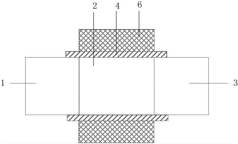
The invention belongs to the field of a logic device and circuit in the field of a super-large-scale integrated circuit, specifically a tunnel field effect transistor with an increased on state current. According to the tunnel field effect transistor, a low K dielectric area is arranged between a source area and a drain area, thereby isolating the source area and the drain area; an intrinsic area is arranged on the source area; a layer of conductive channel is arranged between the intrinsic area and the drain area; and the conductive channel is located on the low K dielectric area. According to the structure of the tunnel field effect transistor, the bipolar effect of a traditional transverse TFET is weakened. Through utilization of a low K dielectric, the contact between the drain area and the intrinsic area is reduced and the bipolar effect is weakened, thereby facilitating thorough switch-off of a device. An electric field of a tunnel junction area is increased by employing the low K dielectric and a high K side wall. The on state current of the TFET is increased through adoption of the side wall (a passivation layer) made of a high dielectric material. According to the tunnel field effect transistor, the bipolar effect is weakened, the on state current is increased, the tunnel field effect transistor is compatible with a CMOS technology and the cost is low.

Description

technical field [0001] The invention belongs to the field of logic devices and circuits in the field of ultra-large-scale integrated circuits, and relates to a longitudinal tunneling TFET device with small size and increased on-state current, in particular to a tunneling field-effect transistor with increased on-state current. Background technique [0002] With the advancement of lithography, implantation and other process technologies, the integration of chips is getting higher and higher, and the power consumption density is also increasing; moreover, the feature size of MOSFET devices is getting smaller and smaller, and the short channel effect, GIDL (gate induced Drain leakage current) becomes severe, further increasing the off-state current. Therefore, the solution to the power consumption problem directly affects the improvement of chip integration. [0003] Finding a device structure with small leakage is the most direct way to solve the static power consumption prob...

Claims


Application Information

Patent Timeline
IPC IPC(8): H01L29/739H01L21/331
CPCH01L29/7391H01L29/66356
Inventor 王向展曹建强马阳昊夏琪李竟春
Owner UNIV OF ELECTRONICS SCI & TECH OF CHINA
Learn More