A stacked high temperature annealing process

A high-temperature annealing and stacking technology, applied in the manufacture of electrical components, circuits, semiconductor/solid-state devices, etc., can solve the problems of fragile silicon wafer carrying devices, easy surface contamination, and easy edge chipping, etc., to improve quality and Qualification rate, reduction of boat loading and unloading time, and large efficiency improvement

A high-temperature annealing and stacking technology, applied in the manufacture of electrical components, circuits, semiconductor/solid-state devices, etc., can solve the problems of fragile silicon wafer carrying devices, easy surface contamination, and easy edge chipping, etc., to improve quality and Qualification rate, reduction of boat loading and unloading time, and large efficiency improvement

CN106257625BActive Publication Date: 2019-02-05HENGDIAN GRP DMEGC MAGNETICS CO LTD

Image

  • A stacked high temperature annealing process
  • A stacked high temperature annealing process
  • A stacked high temperature annealing process

Examples


Embodiment 1

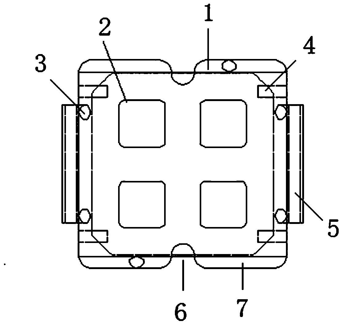
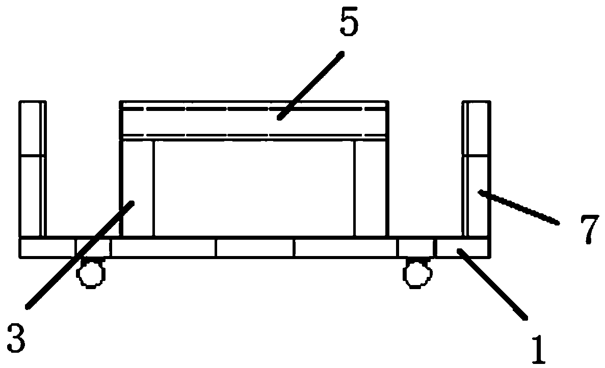
[0033] (1) Stack the etched M2 monocrystalline silicon wafers neatly in a manner of 100 pieces / stack, and put them into the quartz wafer holder for annealing;

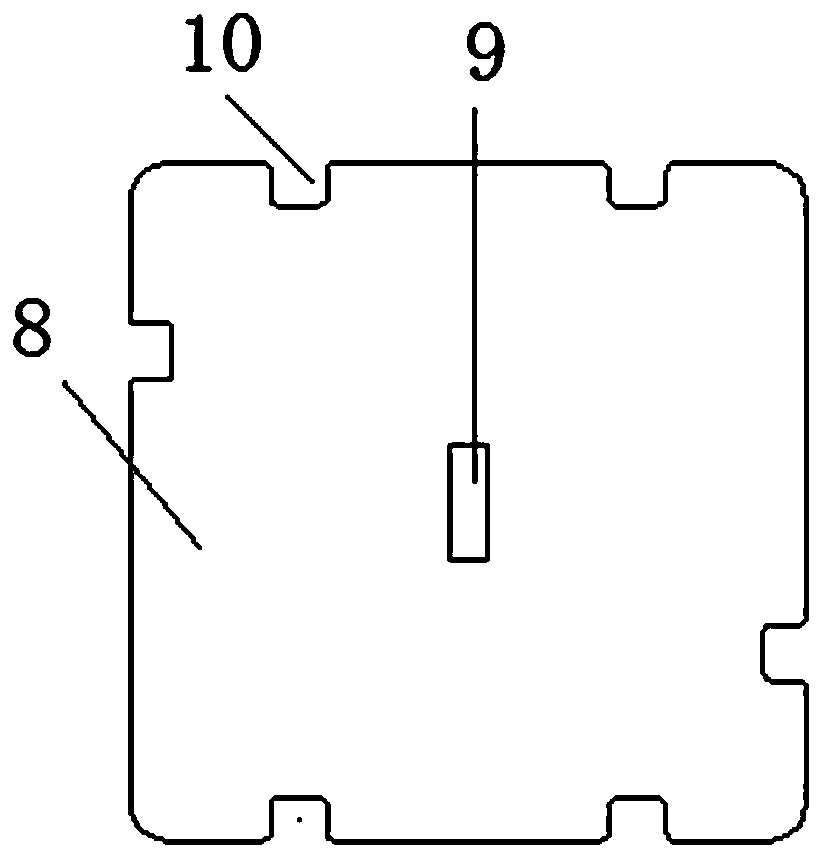
[0034] (2) Cover the silicon chip of the quartz chip frame with a quartz cover plate and press the silicon chip, and send the quartz chip frame into a high-temperature diffusion / oxidation furnace;

[0035] (3) The furnace tube of the high-temperature diffusion / oxidation furnace is heated and stabilized to 650° C., annealed, and the holding time is 20 minutes, and nitrogen gas of 20000 sccm is introduced;

[0036] (4) Cooling out of the furnace: cool down the furnace tube of the high-temperature diffusion / oxidation furnace to 600° C., hold for 600 s, and then out of the furnace.

[0037] After cooling, test the square resistance. At the same time, the traditional high-temperature annealing process was used to process the etched M2 single crystal silicon wafer, and after cooling, the square resistance was tested.

[00...


PUM


Abstract

The invention discloses a stackable high-temperature annealing technology. The technology comprises the following specific operation steps that 1, etched silicon wafers are stacked in order and put into a quartz sheet frame for annealing; 2, the silicon wafers on the quartz sheet frame are covered with a quartz cover plate and pressed, and the quartz sheet frame is fed into a high-temperature diffusion-oxidation furnace; 3, annealing is conducted by increasing and stabilizing the temperature of a furnace tube of the high-temperature diffusion-oxidation furnace; 4, temperature decreasing and discharging from the furnace are conducted, wherein the temperature of the furnace tube of the high-temperature diffusion-oxidation furnace is decreased, and the quartz sheet frame is discharged from the furnace. The stackable high-temperature annealing technology has the advantages that the surfaces of the stacked silicon wafers are isolated from air, and therefore the problems existing in a thermal oxidation technology are effectively solved; operation is easy, the consumed time is short, and quantity production is easy to achieve; meanwhile, the yield is high, the battery piece efficiency is significantly improved, the problems such as edge breakage, corner faults, hidden cracks and fragments in the loading and unloading process of the silicon wafers can be effectively solved, the loading and unloading time is shortened, the quality of battery pieces is improved, and the qualified rate of the battery pieces is increased.

Description

technical field [0001] The present invention relates to the technical field related to photovoltaics, in particular to a stacked high-temperature annealing process. Background technique [0002] Among silicon solar cells, monocrystalline silicon solar cells have the highest conversion efficiency and the most mature technology. Monocrystalline silicon cells show excellent performance due to high-quality monocrystalline silicon materials and advanced processing technology. [0003] Among them, diffusion is one of the key processes in the production process of crystalline silicon solar cells. It is to change the surface of P-type silicon wafers into N-type after diffusion, thereby forming a P-N junction, and silicon wafers have photovoltaic effects. Diffusion needs to use a silicon chip holding device to place the silicon chip on the device, and then place the silicon chip carrying device on the carbonization paddle and send it into the diffusion furnace for concentrated diffu...

Claims


Application Information

Patent Timeline
05 Feb 2019
Publication
CN106257625B
IPC
H01L21/324
CPC
H01L21/324
Inventors
孙涌涛; 彭兴