Thin film resistor and fabrication method thereof
A technology of thin film resistors and resistive layers, applied in the direction of thin film resistors, resistance manufacturing, resistors, etc., can solve the problems of increasing manufacturing costs and reducing surface roughness
- Summary
- Abstract
- Description
- Claims
- Application Information
AI Technical Summary
Problems solved by technology
Method used
Image

Examples
Embodiment 1
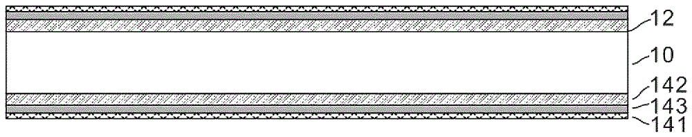
[0080] This embodiment relates to a metal thin film resistor.
[0081] First, glass with a thickness of 500 μm is selected as the substrate. Then, a resistance layer is formed on the surface of the glass substrate by adopting a treatment method of ion implantation followed by plasma deposition.
[0082] In the ion implantation process, one of Ti, Ta, Cr, Ni, Al, Cu, Ag, Au, V, Zr, Mo, Nb, In, Sn, Tb, Be, Ca, Mg is selected as the target material; Preferably, Ni or Cr can be selected as the vacuum cathode arc target material. Control the process temperature of ion implantation to 600°C, vacuumize to 2×10 -1 up to 5×10 -5 Pa, and adjust the energy of the implanted ions to 50-100keV, and the implanted dose is 1.0×10 17 to 5.0×10 17 ion / cm 2 , so that the lower surface of the ion implantation layer is located at a depth of 5-50 nm below the surface of the substrate.
[0083] In the plasma deposition process, one of Ti, Ta, Cr, Ni, Al, Cu, Ag, Au, V, Zr, Mo, Nb, In, Sn, Tb, ...
Embodiment 2
[0085] This embodiment relates to an alloy thin film resistor.
[0086] First, a silicon plate with a thickness of 80 μm is selected as the substrate. Then, a resistance layer is formed on the surface of the silicon plate by using a treatment method of ion implantation followed by plasma deposition. In the process of ion implantation and plasma deposition, the composition of the alloy target material used is shown in Table 1 below, where the values represent mass percentages.
[0087] components Ni Cr Al Ti Cu be Ta Au Alloy combination 1 50 50 Alloy combination 2 40 40 20 Alloy combination 3 47 47 6 Alloy Set 4 75 15 10 Alloy combination 5 50 50 Alloy Set 6 30 20 15 10 25 Alloy combination 7 40 40 20 Alloy combination 8 20 15 20 25 20
[0088] Preferably, during the ion implantation process, a Ni-Cr-Au all...
Embodiment 3
[0091] This embodiment relates to an alloy thin film resistor.
[0092] First, silicon dioxide with a thickness of 100 μm is selected as the substrate. Then, a resistance layer is formed on the surface of the silicon dioxide substrate by using a treatment method of ion implantation followed by plasma deposition.
[0093] In the process of ion implantation, different proportions of Ni-Cr alloys are selected and mixed with Ta, Al or Mo as the vacuum cathode arc target. Preferably, a Ni-Cr-dopant series alloy with a mass ratio of 40:40:20 or 35:55:10 is selected as the vacuum cathode arc target material, and the process temperature of ion implantation is controlled to be 600°C, and the vacuum is evacuated to 2 ×10 -1 up to 5×10 -5 Pa, and the energy of implanted ions is adjusted to 50 to 100keV, and the implanted dose is 1.0×10 17 to 5.0×10 17 ion / cm 2 , so that the lower surface of the ion implantation layer is located at a depth of 5-50 nm below the surface of the substra...
PUM
| Property | Measurement | Unit |
|---|---|---|
| thickness | aaaaa | aaaaa |
| thickness | aaaaa | aaaaa |
| thickness | aaaaa | aaaaa |
Abstract
Description
Claims
Application Information
 - R&D
- Intellectual Property
- Life Sciences
- Materials
- Tech Scout
- Unparalleled Data Quality
- Higher Quality Content
- 60% Fewer Hallucinations
Browse by: Latest US Patents, China's latest patents, Technical Efficacy Thesaurus, Application Domain, Technology Topic, Popular Technical Reports.
© 2025 PatSnap. All rights reserved.Legal|Privacy policy|Modern Slavery Act Transparency Statement|Sitemap|About US| Contact US: help@patsnap.com