Heterojunction solar cell and manufacturing method thereof
A solar cell and heterojunction technology, which is applied in the field of solar cells, can solve the problems of reducing the open circuit voltage of the battery, increasing the series resistance of the battery, and decreasing the conversion efficiency of the battery, and achieves the effect of increasing the open circuit voltage, reducing the series resistance and suppressing bombardment.
- Summary
- Abstract
- Description
- Claims
- Application Information
AI Technical Summary
Problems solved by technology
Method used
Image

Examples
preparation example Construction
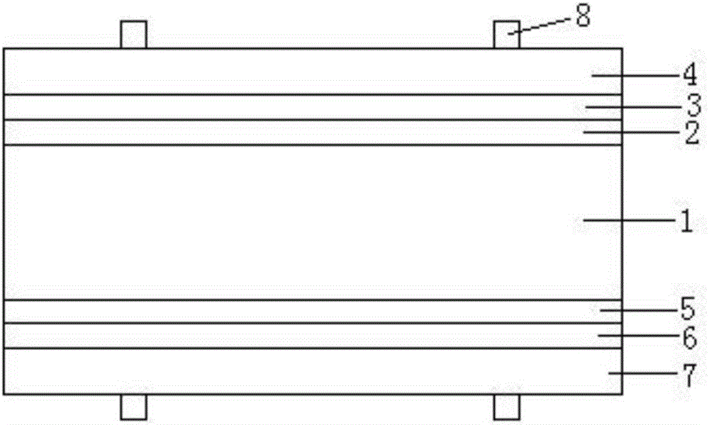
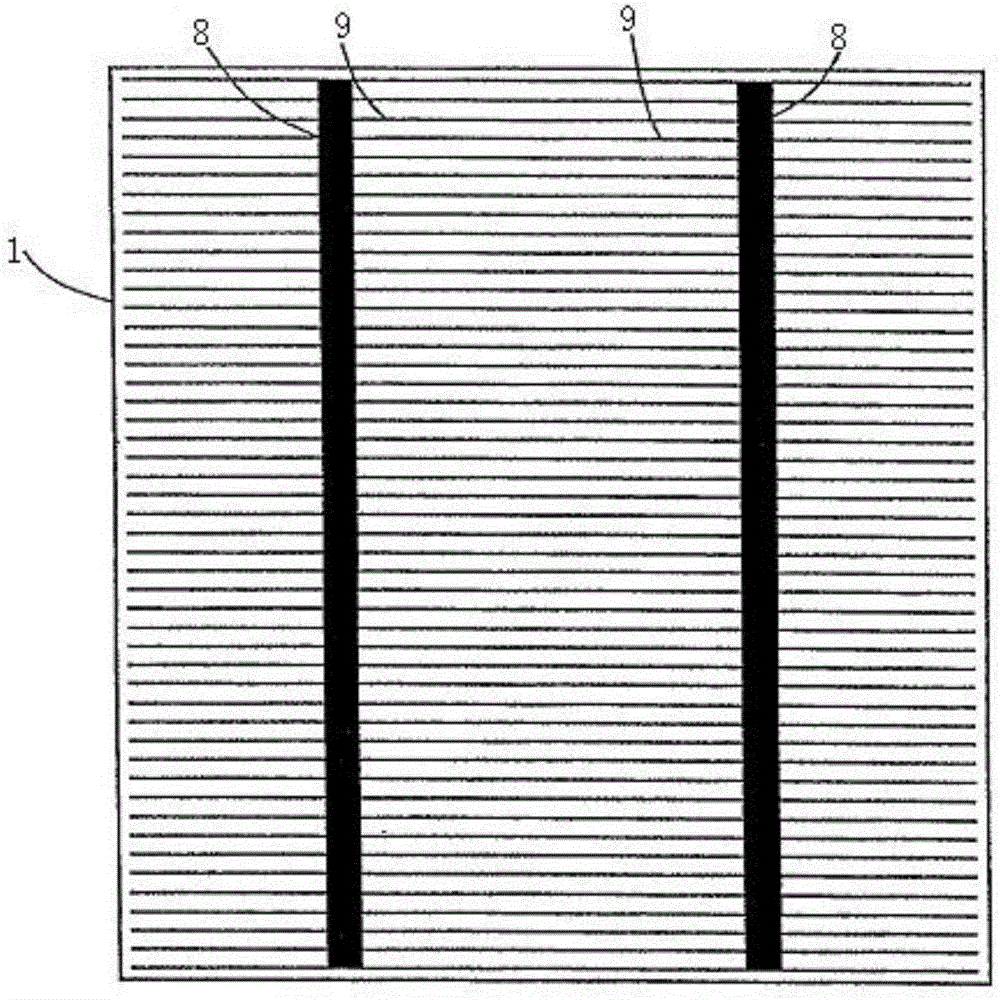
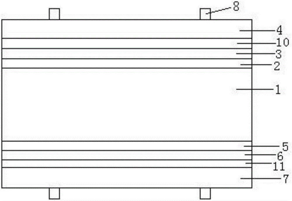
[0060] The preparation method includes: preparing a crystalline silicon substrate 1; depositing a first intrinsic amorphous layer 2 on the light-receiving surface of the crystalline silicon substrate 1; depositing a second intrinsic amorphous layer 5 on the back of the substrate 1 Depositing a first doped layer 3 on the first intrinsic amorphous layer 2; depositing a second doped layer 6 on the second intrinsic amorphous layer 5; depositing a second doped layer 6 on the first doped layer 3 depositing a first doped titanium oxide film layer 10; depositing a first transparent conductive layer 4 on the first doped titanium oxide film layer 10; depositing a second doped titanium oxide film layer on the second doped layer 6 film layer 11; depositing a second transparent conductive layer 7 on the second doped titanium oxide film layer 11; printing a gate electrode 9 on the first transparent conductive layer 4 and the second transparent conductive layer 7.
[0061] Specifically, CVD ...
Embodiment 1
[0068] Prepare an N-type monocrystalline silicon wafer 1 with a thickness of 200um, and then sequentially deposit 8nm intrinsic amorphous silicon film layers on the light-receiving surface of the N-type monocrystalline silicon wafer 1 as the first intrinsic amorphous layer 2 and A 20nm p-type amorphous silicon film layer is used as the first doped layer 3; then an 8nm intrinsic amorphous silicon film layer is sequentially deposited on the back of the n-type single crystal silicon wafer 1 by PECVD method as the second intrinsic amorphous silicon film layer. The n-type amorphous silicon film layer of layer 5 and 30nm is used as the second doped layer 6; then adopts RPD method to deposit 10nm TiO on the p-type amorphous silicon film layer 3 2 : W film layer 10; followed by magnetron sputtering on TiO 2 : Deposit an 80nm ITO film layer on the W film layer 10 as the first transparent conductive layer 4; then use the RPD method to deposit 10nm TiO on the n-type amorphous silicon fil...
Embodiment 2
[0070] Prepare an N-type monocrystalline silicon wafer 1 with a thickness of 180um, and then sequentially deposit 10nm intrinsic amorphous silicon film layers on the light-receiving surface of the N-type monocrystalline silicon wafer 1 as the first intrinsic amorphous layer 2 and A 20nm p-type amorphous silicon film layer is used as the first doped layer 3; then a 10nm intrinsic amorphous silicon film layer is sequentially deposited on the back of the n-type single crystal silicon wafer 1 by PECVD method as the second intrinsic amorphous silicon film layer. The n-type amorphous silicon film layer of layer 5 and 30nm is used as the second doped layer 6; then adopts RPD method to deposit 10nm TiO on the p-type amorphous silicon film layer 3 2 : Nb film layer 10; followed by magnetron sputtering on TiO 2 : Deposit an 80nm ITO film layer on the Nb film layer 10 as the first transparent conductive layer 4; then use the RPD method to deposit 10nm TiO on the n-type amorphous silicon ...
PUM
| Property | Measurement | Unit |
|---|---|---|
| thickness | aaaaa | aaaaa |
| thickness | aaaaa | aaaaa |
| thickness | aaaaa | aaaaa |
Abstract
Description
Claims
Application Information
 - R&D
- Intellectual Property
- Life Sciences
- Materials
- Tech Scout
- Unparalleled Data Quality
- Higher Quality Content
- 60% Fewer Hallucinations
Browse by: Latest US Patents, China's latest patents, Technical Efficacy Thesaurus, Application Domain, Technology Topic, Popular Technical Reports.
© 2025 PatSnap. All rights reserved.Legal|Privacy policy|Modern Slavery Act Transparency Statement|Sitemap|About US| Contact US: help@patsnap.com