Vacuum film-plating process for gate pattern of semiconductor chip shielded by mask at high accuracy

A processing technology and semiconductor technology, which can be used in vacuum evaporation plating, photoengraving process exposure devices, semiconductor/solid-state device manufacturing, etc., and can solve the problems of secondary metal film blistering, silver flakes shifting, and falling off.

Active Publication Date: 2017-01-11
西安派瑞功率半导体变流技术股份有限公司
View PDF6 Cites 0 Cited by
  • Summary
  • Abstract
  • Description
  • Claims
  • Application Information

AI Technical Summary

Problems solved by technology

The first photolithography and the first chemical etching process mostly use photoresist, strong acid, strong alkali and other chemical materials, which can easily cause pollution to the semiconductor chip and the first vacuum coating layer. If the pretreatment of the second vacuum coating film is not Clean, it is very easy to cause the second metal film to bubble, fall off, and lack of film, which will seriously affect the performance of the device
[0006] 3. Repeated use of photolithography mask and chemical etching process will increase the difficulty of the process, and will introduce cumulative errors, so that the gate-cathode isolation cannot be reliably controlled, and the yield rate will drop significantly
The disadvantage is that the longitudinal silver sheet cannot be processed very thinly, so the longitudinal isolation distance is very wide, and because the contact between the silver sheet and the metal film layer is layer-to-layer, rather than intimate contact between atoms, the gap between the two layers Failure to form a good ohmic contact between them will cause large longitudinal resistance and large transient thermal impedance, which will seriously affect the performance of the device; in severe cases, the silver sheet may also move, short-circuit with the gate metal film, and cause the thyristor to burn out

Method used


Image

  • Vacuum film-plating process for gate pattern of semiconductor chip shielded by mask at high accuracy
  • Vacuum film-plating process for gate pattern of semiconductor chip shielded by mask at high accuracy
  • Vacuum film-plating process for gate pattern of semiconductor chip shielded by mask at high accuracy

Examples


Embodiment Construction

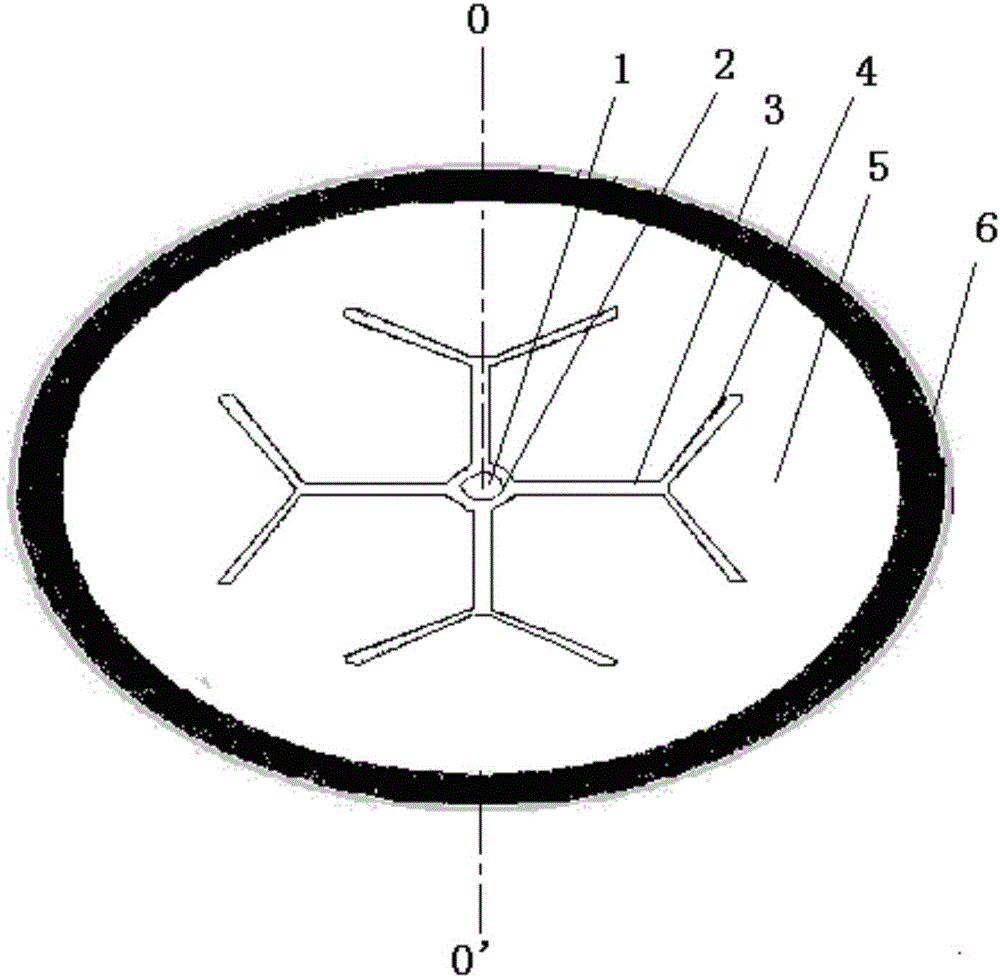
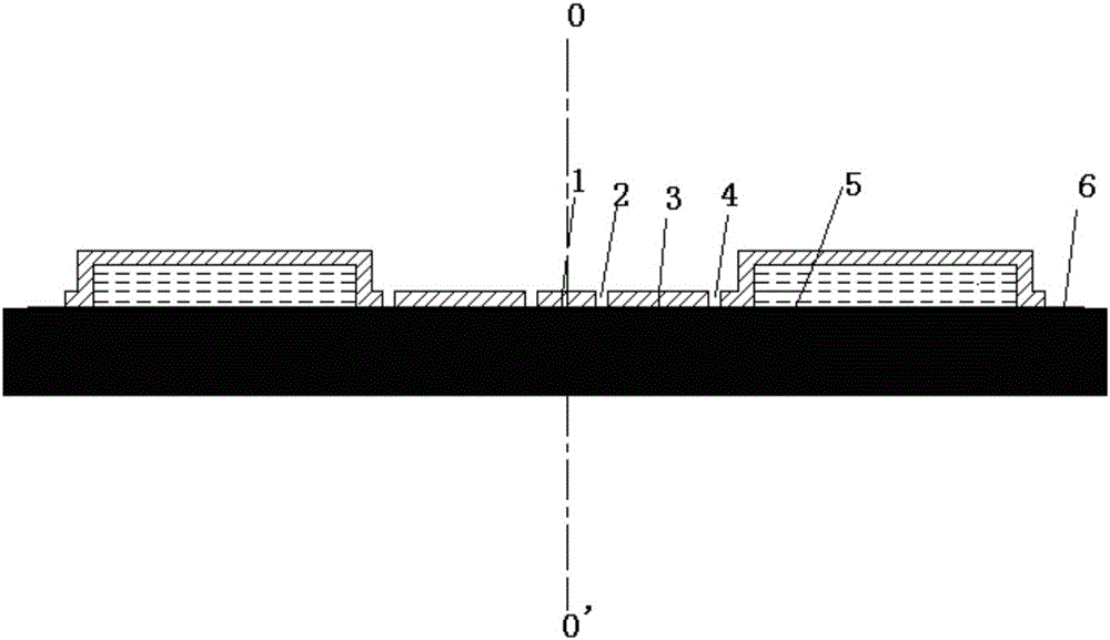
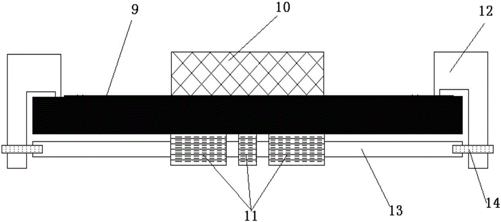
[0031] Such as Figure 1-7 As shown, the high-power thyristor semiconductor device includes a semiconductor chip 9, and the semiconductor chip 9 is provided with a central gate pattern 1, an enlarged gate pattern 3, a cathode pattern 5 and a mesa pattern 6. The first layer of metal film 8 is distributed on the cathode pattern 5 on the semiconductor chip 9; the second layer of metal film 7 is distributed on the first layer of the central gate pattern 1 and the enlarged gate pattern 3 and cathode pattern 5 on the semiconductor chip 9 On the metal film 8; the central gate pattern 1 metal film and the enlarged gate pattern 3 metal film are separated by the isolation line 2; the enlarged gate pattern 3 metal film and the cathode pattern 5 metal film are separated by the isolation line 4, and the cathode pattern 5 metal can be seen The film is composed of a first layer of metal film 8 and a second layer of metal film 7; the second layer of metal film 7 has good ohmic contact with th...


PUM

PropertyMeasurementUnit
electrical resistivityaaaaaaaaaa
thicknessaaaaaaaaaa
thicknessaaaaaaaaaa

Abstract

The invention provides a vacuum film-plating process for a gate pattern of a semiconductor chip shielded by a mask at high accuracy. The vacuum film-plating process is characterized in that a gate mask is aligned with the gate electrode of the semiconductor chip at high accuracy; the gate mask is fixed by a high-temperature-resistant strong magnet; and technological methods of secondary vacuum film plating, primary photoetching and primary chemical corrosion are adopted. Through adoption of the vacuum film-plating process, a large quantity of raw materials are saved; a production period is shortened; and process error accumulation caused by repeated photoetching and chemical corrosion is eliminated at the same time. The vacuum film-plating process has the advantages of simple technological methods, short production period, high production accuracy, reliability, easiness in control, saving of raw materials, superior device performance, high product yield and the like. The vacuum film-plating process plays a role in revolutionarily prompting a vacuum film-plating technology for a high-power thyristor semiconductor chip. Through adoption of the vacuum film-plating process, the yield is increased greatly, and a tremendous economic benefit is achieved.

Description

technical field [0001] The invention relates to the technical field of power semiconductor device manufacturing, in particular to a high-power thyristor semiconductor chip vacuum coating film contact process. Background technique [0002] As we all know, in a high-power thyristor semiconductor chip, there are three electrodes: anode, cathode and gate. Adding a positive trigger signal between the gate and cathode can control the conduction of the thyristor; adding a negative trigger signal between the gate and cathode can control the turn-off of the thyristor. The gate and the cathode are on the same side of the semiconductor chip, and both are integrated with semiconductor integrated circuit elements. The surface of the integrated circuit element needs to be covered with a metal film, and the metal film is used as the ohmic contact of the internal electrode and the lead between the integrated circuit elements. Isolation must be realized between the metal film covering the s...

Claims


Application Information

Patent Timeline
Patent Type & Authority Applications(China)
IPC IPC(8): H01L21/027H01L21/02C23C14/24G03F7/20
CPCC23C14/24G03F7/20H01L21/02041H01L21/027
Inventor 高山城郭永忠马宁强赵卫赵涛
Owner 西安派瑞功率半导体变流技术股份有限公司
Why Eureka
Try Eureka