Preparation method of vertical-structure purple light LED chip

An LED chip, vertical structure technology, applied in electrical components, circuits, semiconductor devices, etc., can solve the problems of restricting the working current of LED chips, working current limitation, long heat conduction path, etc., to improve photoelectric efficiency, device efficiency, The effect of improved heat dissipation

Active Publication Date: 2017-01-11
CHINA UNITED NORTHWEST INST FOR ENG DESIGN & RES
View PDF4 Cites 3 Cited by
  • Summary
  • Abstract
  • Description
  • Claims
  • Application Information

AI Technical Summary

Problems solved by technology

Therefore, this P-type contact structure restricts the working current of the LED chip
On the other hand, the PN junction heat of this structure is exported through the sapphire substrate. In view of the low thermal conductivity of sapphire, the heat conduction path is longer for large-sized power chips, and the thermal resistance of this LED chip is relatively large. current is also limited

Method used


Image

  • Preparation method of vertical-structure purple light LED chip
  • Preparation method of vertical-structure purple light LED chip
  • Preparation method of vertical-structure purple light LED chip

Examples


preparation example Construction

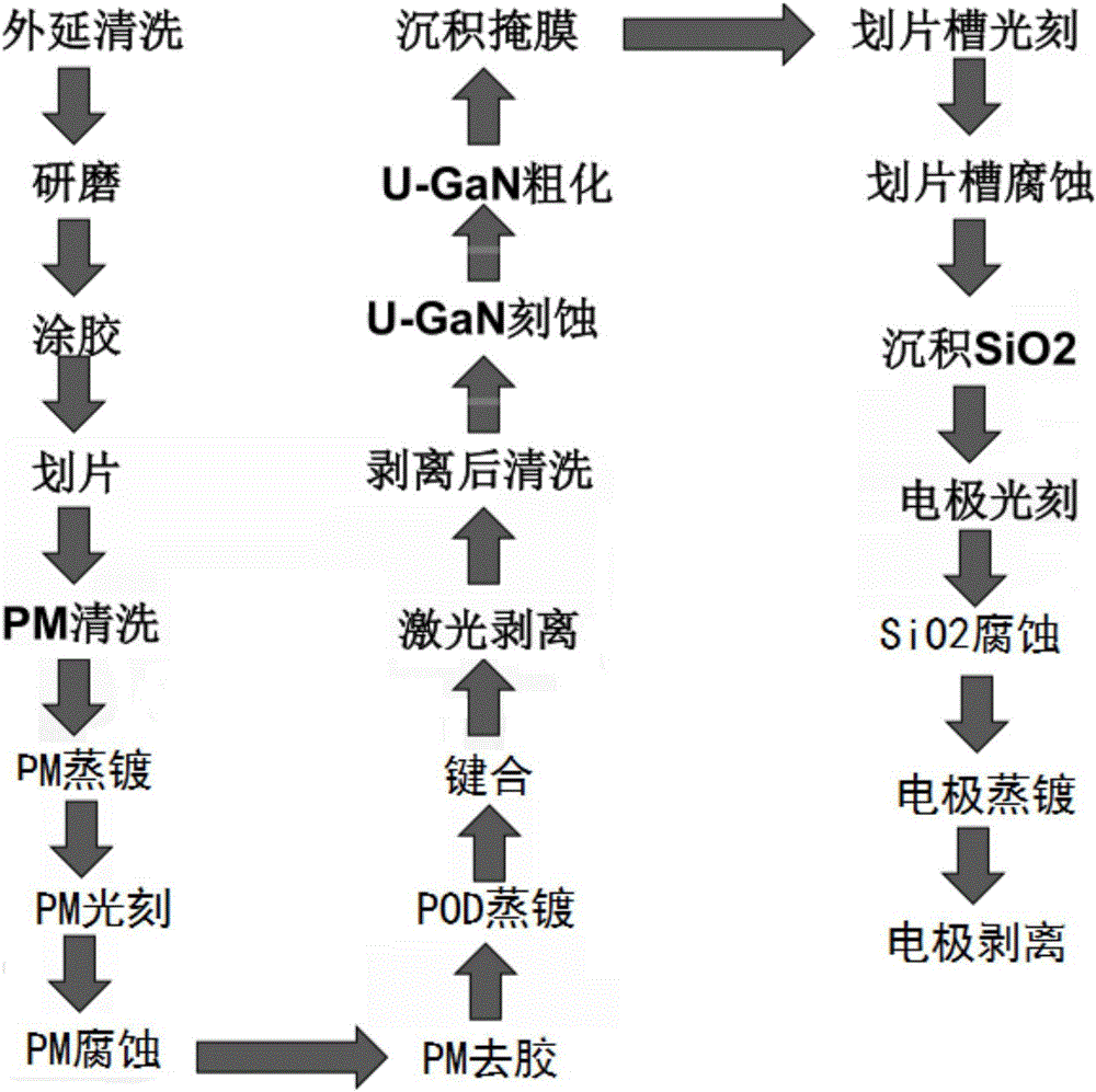
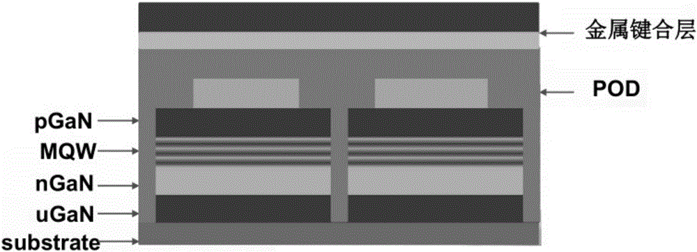
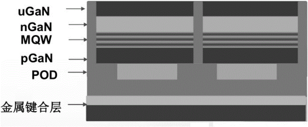
[0056] see figure 1 As shown, the present invention discloses a method for preparing a vertical structure violet LED chip. The substrate with a low-temperature u-GaN repair layer and substrate is used as the growth base, and then other layers are sequentially grown on the flat u-GaN surface Epitaxy, to prepare the purple LED epitaxial wafer; finally, the purple LED epitaxial wafer is made into a vertical structure LED, which mainly includes the following steps: depositing a reflector on the surface of the LED epitaxial wafer, and making a metal electrode pattern, using a high temperature metal bonding process. The surface of the metal electrode pattern is bonded on the metal substrate, and the substrate is peeled off by laser lift-off technology; another metal electrode pattern is made on the surface of u-GaN.

[0057] The bonding process is to prepare the bonding layer material on the surface of the wafer to be bonded, then stick the two wafers together and use external energ...

Embodiment 1

[0080] First prepare the purple LED epitaxial wafer, including the following steps:

[0081] 1.1) Pass N at a temperature of 1070°C and a pressure of 150torr 2 Baking for 10 minutes, nitrided sapphire, SiC or Si substrate, the substrate thickness is 430μm;

[0082] 1.2) Cool down the sapphire, SiC or Si substrate after nitriding in step 1.1 to 515°C and a pressure of 800torr, then grow a substrate with a thickness of 15nm on the substrate, then raise the temperature to 1030°C and a pressure of 400torr to recrystallize the substrate , and then grow a 1.8μm u-GaN repair layer;

[0083] 1.3) Raise the temperature to 1070°C and the pressure is 200torr to grow a lightly Si-doped n-GaN layer with a thickness of 500nm, and then grow a heavily Si-doped n-GaN layer with a thickness of 300nm;

[0084] 1.4) growing an n-AlGaN current spreading layer on the basis of the heavily Si-doped n-GaN layer, with a thickness of 80 nm;

[0085] 1.5) On the basis of the n-AlGaN layer, grow a Si-dop...

Embodiment 2

[0102] First prepare the purple LED epitaxial wafer, including the following steps:

[0103] 1.1) Pass N at a temperature of 1080°C and a pressure of 150torr 2 Baking for 20 minutes, nitrided sapphire, SiC or Si substrate, the substrate thickness is 440μm;

[0104] 1.2) Cool down the sapphire, SiC or Si substrate after nitriding in step 1 to 525°C and a pressure of 800torr, then grow a substrate with a thickness of 25nm on the substrate, then raise the temperature to 1040°C and a pressure of 400torr to recrystallize the substrate , and then grow a 2.1μm u-GaN repair layer;

[0105] 1.3) Raise the temperature to 1080°C and the pressure to 200torr to grow a lightly Si-doped n-GaN layer with a thickness of 550nm, and then grow a heavily Si-doped n-GaN layer with a thickness of 350nm;

[0106] 1.4) growing an n-AlGaN current spreading layer on the basis of the heavily Si-doped n-GaN layer, with a thickness of 160 nm;

[0107] 1.5) On the basis of the n-AlGaN layer, grow a Si-do...


PUM


Abstract

The invention discloses a preparation method of a vertical-structure purple light LED chip. The preparation method is characterized by taking a substrate provided with a low-temperature u-GaN repairing layer and a base as a growth foundation, then sequentially growing epitaxies of other layers at the smooth surface of the u-GaN repairing layer so as to acquire a purple light LED epitaxial wafer; and finally preparing the purple light LED epitaxial wafer into a vertical-structure LED. The process of preparing the purple light LED epitaxial wafer into an LED with a vertical structure mainly comprises the steps of performing deposition at the surface of the LED epitaxial wafer to form a reflector, preparing a metal electrode pattern, bonding the surface of the metal electrode pattern to a metal base plate by using a high-temperature metal bonding technology, and de-bonding the substrate by using a laser de-bonding technology; preparing another metal electrode pattern at the surface of the u-GaN repairing layer. The prepared vertical-structure LED single chip is high in power, the number of series-parallel connection LEDs is reduced, and user requirements can be met by the single chip. Meanwhile, the design of a driving circuit is simplified, and reliability of an LED product is greatly improved, and the service life of the LED product is greatly prolonged.

Description

[0001] 【Technical field】 [0002] The invention belongs to the technical field of semiconductors, and in particular relates to a method for preparing a vertical structure violet LED chip. [0003] 【Background technique】 [0004] The application of semiconductor lighting has accelerated significantly in recent years, and its effect has been recognized by the market, but its penetration rate in the entire lighting market is still low. The domestic LED lighting application market has not yet become the leading force in industrial development. The semiconductor lighting application market, especially the functional lighting market is in the initial stage of development, with huge future space. [0005] For traditional front-mounted LED chips, P-type GaN is difficult to dope, resulting in low hole carrier concentration and difficulty in growing thick, resulting in difficult diffusion of current. At present, the method of preparing ultra-thin metal film or ITO film on the surface of...

Claims


Application Information

Patent Timeline
Patent Type & Authority Applications(China)
IPC IPC(8): H01L33/00H01L33/06H01L33/12H01L33/24H01L33/32H01L33/62H01L33/64
CPCH01L33/0075H01L33/0093H01L33/06H01L33/12H01L33/24H01L33/32H01L33/62H01L33/641
Inventor 田伟刘波波田进赵俊李谊
Owner CHINA UNITED NORTHWEST INST FOR ENG DESIGN & RES
Why Eureka
Try Eureka