Manufacturing method of silicon-based MEMS micro nano through hole structure

A manufacturing method and a technology of through-silicon vias, which are applied in the direction of microstructure technology, microstructure devices, and manufacturing microstructure devices, etc., can solve the problems of unsuitability for large-scale micro-nano manufacturing, poor consistency and stability, and complicated thinning and polishing. , to achieve good consistency in different batches, simple steps, and low difficulty in achieving the effect

Inactive Publication Date: 2017-01-18
BEIJING RES INST OF TELEMETRY +1
View PDF5 Cites 7 Cited by
  • Summary
  • Abstract
  • Description
  • Claims
  • Application Information

AI Technical Summary

Problems solved by technology

In order to solve this problem, the method adopted by Yu Yuanwei and ZHU Jian et al. (Yu Yuanwei, ZHANG Yong and ZHU Jian, Monolithic Silicon Micromachined Ka-band Filters. Microwave and MillimeterWave Technology, 2008) of CLP 55 Institute is: select the substrate The thickness of the silicon wafer is greater than the depth of the through hole by a certain value, and the etching depth of DRIE or ICP is slightly larger than the design depth of the through hole, but there is no penetration, and then the back of the substrate wafer is thinned and polished to the designed thickness, but this method is more complicated. In particular, thinning and polishing are more complicated and less efficient, and are not suitable for mass micro-nano manufacturing
Sunil Kumar and William T.Pike of Imperial College of Technology (Sunil Kumar and WilliamT.Pike, Technique for Eliminating Notching in Through-Wafer Etching.16 th MMEMicromechanics Europe Workshop, 2005) proposed an etching method to solve the defect of the back opening of the through hole. The implementation method is: AZ9260 photoresist and aluminum composite film system are selected for the anti-etching mask layer on the front side of the silicon wafer, and aluminum is plated on the back side of the silicon wafer. film, etch for a period of time, take out the silicon wafer and paste it on the bottom bracket with SPR1813 glue when the etching is fast, and then continue to etch until it is over-etched for a certain period of time. The bottom bracket is less consistent and stable

Method used


Image

  • Manufacturing method of silicon-based MEMS micro nano through hole structure
  • Manufacturing method of silicon-based MEMS micro nano through hole structure
  • Manufacturing method of silicon-based MEMS micro nano through hole structure

Examples


Embodiment Construction

[0039] Below in conjunction with accompanying drawing and specific embodiment the present invention is described in further detail:

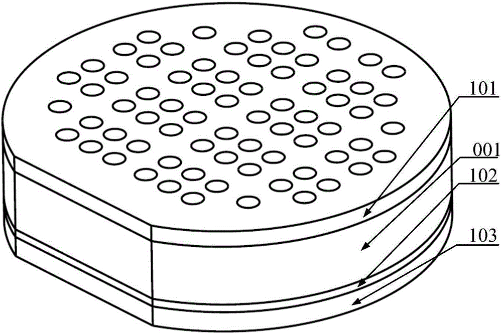
[0040] Such as figure 1 Shown is a schematic diagram of a three-dimensional structure of a silicon MEMS through-hole structure micro-nano implementation method. It can be seen from the figure that a method for manufacturing a silicon-based MEMS micro-nano through-hole structure includes the following steps:

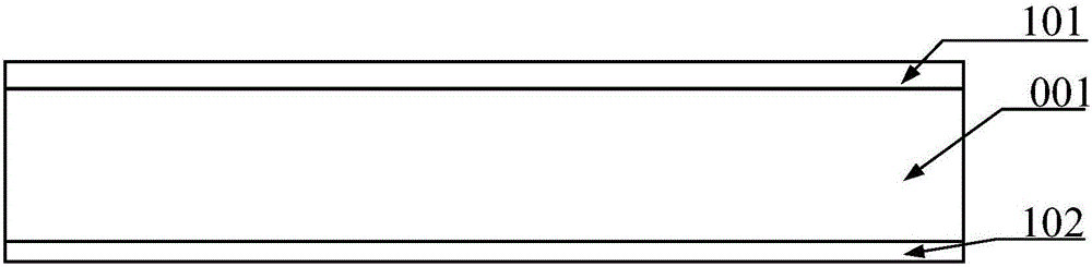
[0041] Step (1), such as figure 2 Shown is a schematic diagram of the steps of depositing a silicon dioxide film / metal film. It can be seen from the figure that a silicon dioxide film layer 101 is grown on the upper surface of the silicon wafer substrate 001, and a silicon dioxide film layer 101 is grown on the lower surface of the silicon wafer substrate 001. Deposit a layer of metal thin film layer 102; wherein, the method for growing silicon dioxide thin film layer 101 is PECVD method, thermal oxidation method or LPCVD method, and the ...


PUM

PropertyMeasurementUnit
thicknessaaaaaaaaaa
thicknessaaaaaaaaaa
thicknessaaaaaaaaaa

Abstract

The invention discloses a manufacturing method of a silicon-based MEMS micro nano through hole structure, and relates to the field of realizing methods of silicon through hole structures. The manufacturing method comprises the following steps: depositing a silicon dioxide thin film on the front surface of a silicon substrate material, then performing through hole graph transferring, depositing a metal thin film layer on the back surface of the silicon substrate material, and coating the back surface of the silicon substrate material with a photoresist thin film layer. The through hole graph transferring of the silicon dioxide thin film is performed by a trifluoromethane RIE dry etching method; a pretreatment step of silicon dry etching comprises oxygen RIE etching cleaning and trifluoromethane RIE dry etching cleaning, and then dry deep etching for silicon is performed; the defects of complicated steps, low efficiency, low consistency, low stability and the like of the conventional method for realizing the silicon micro nano through hole structure by dry etching (DRIE or ICP) are overcome; the novel method for realizing dry etching of micro nano on a silicon through hole structure is provided, so that the realizing efficiency of the micro nano on the silicon through hole structure is greatly improved, and the manufacturing precision, the consistency and the stability are also improved.

Description

technical field [0001] The invention relates to the field of a method for realizing a through-silicon hole structure, in particular to a method for manufacturing a silicon-based MEMS micro-nano through-hole structure. Background technique [0002] Micro-Electro-Mechanical System (MEMS for short), mainly covers micro-nano sensors, micro-nano actuators, micro-nano optical components, micro-nano radio frequency components, micro-nano biochemical bearing structures and other micro-miniature devices and structures . The micro-nano through-hole structure is one of the important basic structural units to realize three-dimensional interconnection integration, radio frequency microwave passive devices, and biochemical specific micro-nano structures. Its accuracy, shape integrity, side wall smoothness and steepness are critical It affects the performance index of the final device, and its realization efficiency, consistency, stability, etc. affect the yield and cost of the final devi...

Claims


Application Information

Patent Timeline
Patent Type & Authority Applications(China)
IPC IPC(8): B81C1/00
CPCB81C1/00087B81C1/00396B81C1/00801
Inventor 焦海龙赵广宏李文博金小锋张世名邹江波
Owner BEIJING RES INST OF TELEMETRY
Why Eureka
Try Eureka