LED epitaxial structure and growing method thereof

An epitaxial structure and growth method technology, applied in the field of electronics, can solve the problems of high Al content in the electron blocking layer, discontinuous energy band bending, and unfavorable hole injection, so as to achieve increased hole injection efficiency, improved crystal quality, and convenient parameters. The effect of control

Inactive Publication Date: 2017-02-08
XIANGNENG HUALEI OPTOELECTRONICS
View PDF4 Cites 7 Cited by
  • Summary
  • Abstract
  • Description
  • Claims
  • Application Information

AI Technical Summary

Problems solved by technology

[0003] In the prior art, the LED epitaxial structure is detailed in figure 1 , its growth adopts 2-inch or 4-inch sapphire pss substrate or planar substrate. After the GaN epitaxial layer is grown on the light-emitting layer, pAlGaN material or pAlGaN/pInGaN superlattice containing Al and In components ar

Method used


Image

  • LED epitaxial structure and growing method thereof
  • LED epitaxial structure and growing method thereof
  • LED epitaxial structure and growing method thereof

Examples


Embodiment 1

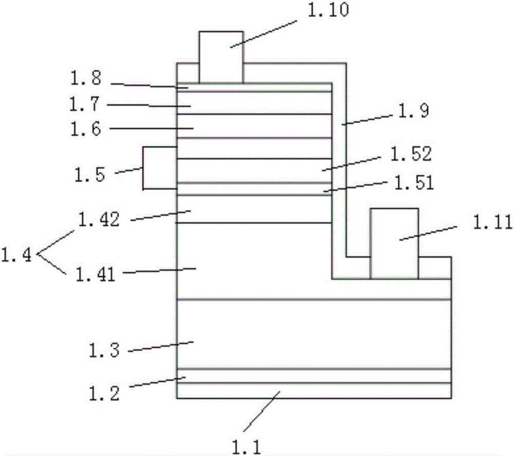
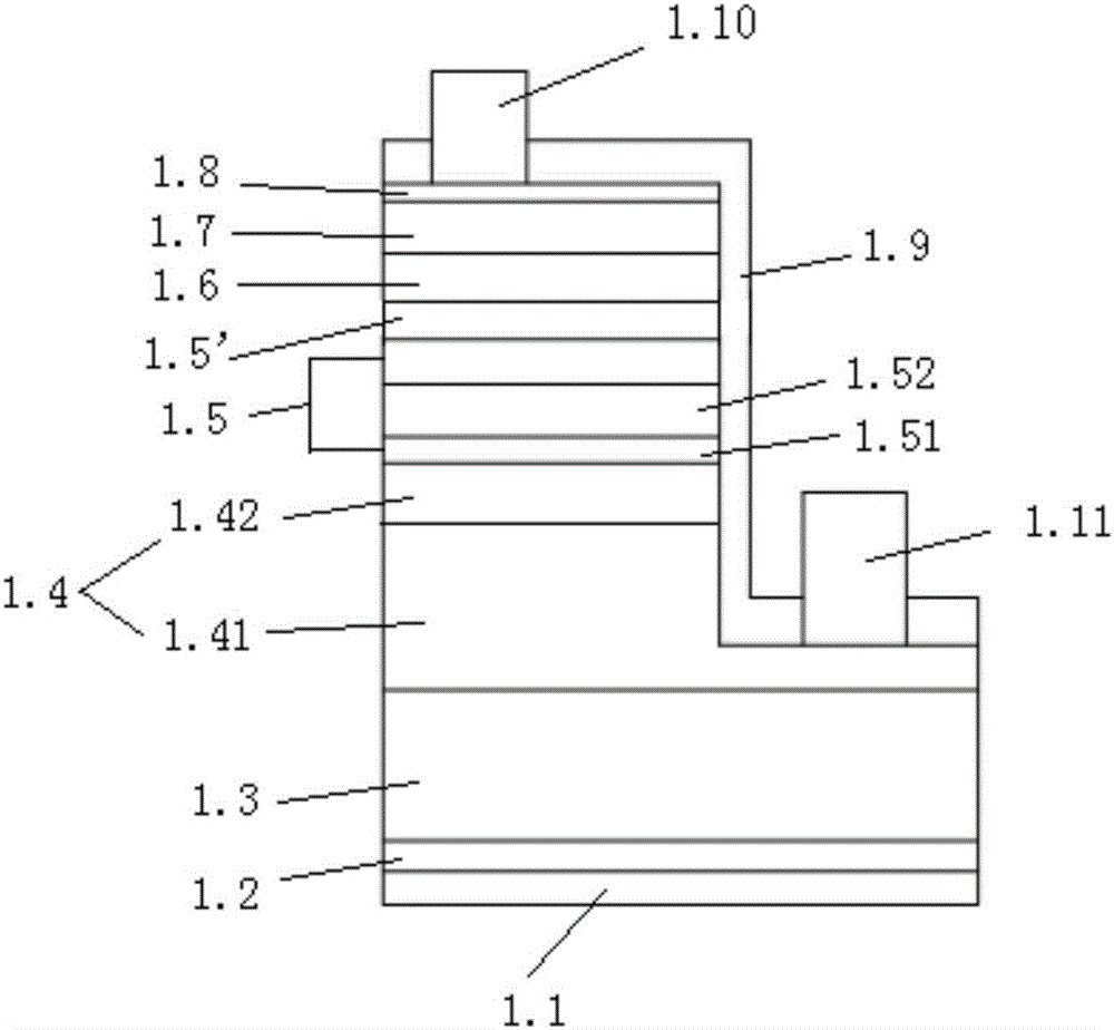
[0050] see figure 2 , an LED epitaxial structure, sequentially stacked sapphire substrate 1.1, low-temperature buffer layer 1.2, undoped GaN layer 1.3, Si-doped n-type GaN layer 1.4, In x Ga (1-x) N / GaN light-emitting layer 1.5, p-type InN layer 1.5', p-type AlGaN layer 1.6 and magnesium-doped p-type GaN layer 1.7.

[0051] The thickness of the low-temperature buffer layer 1.2 is 20-40 nm, and the low-temperature buffer layer 1.2 is corroded into a plurality of irregular small islands.

[0052] The thickness of the undoped GaN layer 1.3 is 2-4 μm.

[0053] The Si-doped n-type GaN layer 1.4 includes a first Si-doped n-type GaN layer 1.41 and a second Si-doped n-type GaN layer 1.42 stacked in sequence, and the first Si-doped n-type GaN layer The thickness of the layer 1.41 is 3-4 μm, and the thickness of the second Si-doped n-type GaN layer 1.42 is 200-400 nm.

[0054] The In x Ga (1-x) The N / GaN light-emitting layer 1.5 includes 7-15 monomers stacked, and the monomers in...

Embodiment 2- Embodiment 3

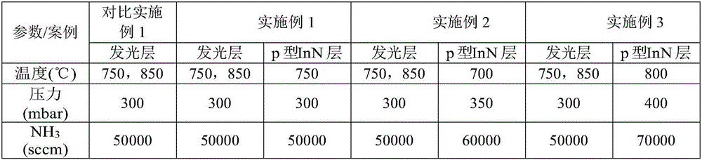
[0072] The difference between embodiment 2-3 and embodiment 1 is the parameters in table 1:

[0073] The part parameter statistical table of table 1 comparative embodiment, embodiment 1-embodiment 3

[0074]

[0075]

[0076] The LED epitaxial structures obtained in Examples 2-3 are marked as S2-S3.


PUM

PropertyMeasurementUnit
Thicknessaaaaaaaaaa
Thicknessaaaaaaaaaa
Thicknessaaaaaaaaaa

Abstract

The invention provides an LED epitaxial structure comprising a sapphire substrate, a low-temperature buffer layer, a non-doped GaN layer, a Si-doped n-type GaN layer, a light emitting layer, a p-type InN layer, a p-type AlGaN layer and a magnesium-doped p-type GaN layer, which are stacked in turn. By arranging the p-type InN layer between the light emitting layer and an electron blocking layer, the following effects are achieved: on one hand, the p-type InN material helps to solve the stress problem properly, a smooth energy band is more suitable for hole injection, the hole injection efficiency is increased, and the light efficiency of LED devices is increased on a macro level; and on the other hand, the p-type InN layer increases the distance between a GaN epitaxial layer and the electron blocking layer and effectively blocks the diffusion of Mg atoms in the electron blocking layer, the concentration of Mg impurity atoms in the light emitting layer is reduced, the crystal quality of the light emitting layer is improved to a certain degree, and the light efficiency of LED devices can be further improved. The invention further discloses a growing method of the LED epitaxial structure, which includes simple steps and is advantageous for industrialization production.

Description

technical field [0001] The invention relates to the field of electronic technology, in particular to an LED epitaxial structure and a growth method thereof. Background technique [0002] At present, LED is a kind of solid-state lighting, which is recognized by consumers because of its advantages such as small size, low power consumption, long service life, high brightness, environmental protection, and durability. The driving voltage and brightness requirements of high-power devices are the focus of current market demand. [0003] In the prior art, the LED epitaxial structure is detailed in figure 1 , its growth adopts 2-inch or 4-inch sapphire pss substrate or planar substrate. After the GaN epitaxial layer is grown on the light-emitting layer, pAlGaN material or pAlGaN / pInGaN superlattice containing Al and In components are directly grown as the electron blocking layer. The layer contains high Al, the electron blocking layer and the GaN epitaxial layer lattice mismatch, ...

Claims


Application Information

Patent Timeline
IPC IPC(8): H01L33/06H01L33/12H01L33/14H01L33/32H01L33/00
CPCH01L33/06H01L33/007H01L33/12H01L33/14H01L33/145H01L33/32
Inventor 张宇
Owner XIANGNENG HUALEI OPTOELECTRONICS
Why Eureka
Try Eureka