

Compound-based semiconductor ultrathin substrate manufacturing method
A production method and compound technology, applied in semiconductor/solid-state device manufacturing, electrical components, circuits, etc., can solve the problems of difficult operation, large error, poor substrate flatness, etc., achieve good thickness controllability, and reduce thickness error , The effect of simple process
- Summary
- Abstract
- Description
- Claims
- Application Information
AI Technical Summary
Problems solved by technology
Method used
Image

Examples
Embodiment Construction
[0038] This embodiment provides a method for thinning a compound semiconductor gallium arsenide substrate, including the following steps:
[0039] (1) The Schottky diode terahertz device is fabricated on the gallium arsenide compound epitaxial material layer;
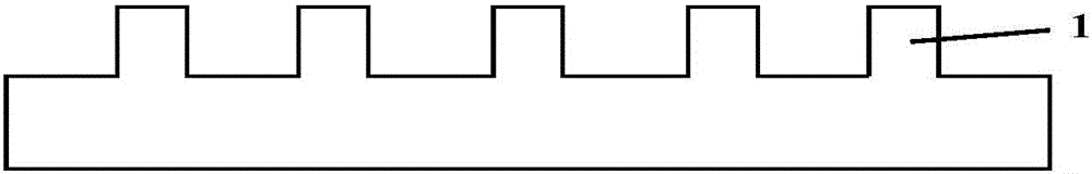
[0040] (2) Use AZ4620 photoresist as a mask to define a deep isolation mesa around the terahertz device, use ICP etching, the etching gas is chlorine and boron trichloride, the etching depth is 6 microns, and remove the glue with acetone , and cleaned with acetone, ethanol, deionized water;
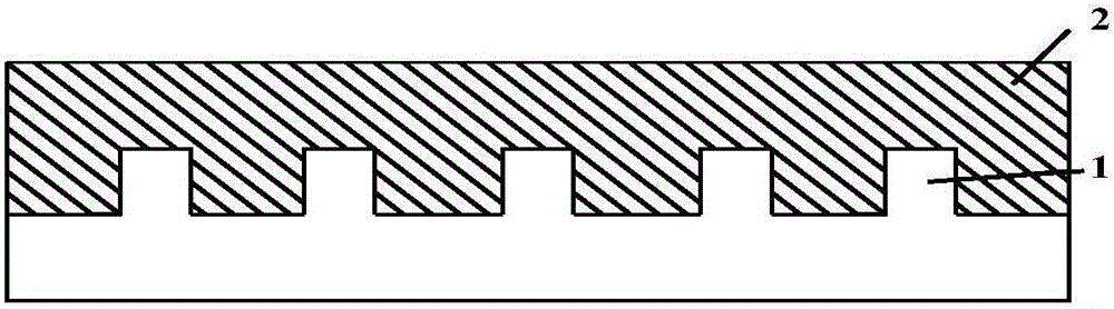
[0041] (3) On the gallium arsenide epitaxial wafer etched with isolation deep grooves, first apply PMMA electron beam photoresist 4 microns, bake at 180 for 2 minutes; then apply PMMA electron beam photoresist 6 microns, 180 degrees hot plate The thickness of the glue was 2 minutes, and a total of 10 microns of PMMA electron beam photoresist was coated on it.
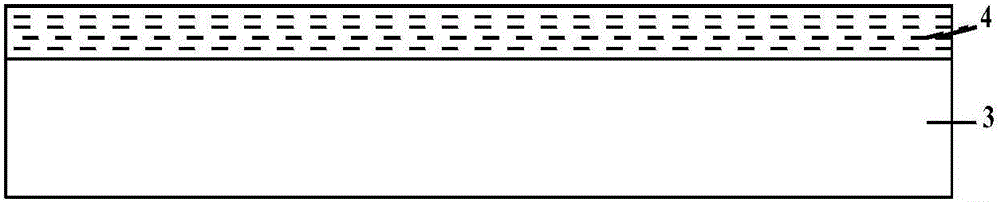
[0042] (4) growing protective medium silicon dioxide 20 nanometers on...
PUM
| Property | Measurement | Unit |
|---|---|---|
| thickness | aaaaa | aaaaa |
Abstract
Description
Claims
Application Information