

Application of metal element-doped ZnO nano material in light-emitting diode
A technology of light-emitting diodes and nanomaterials, which is applied to electrical components, circuits, organic semiconductor devices, etc., can solve the problems of deteriorating the working efficiency of quantum dot light-emitting diodes and reducing the separation of excitons in the quantum dot light-emitting layer, so as to reduce separation and improve work efficiency. Efficiency, effect of reducing process steps
- Summary
- Abstract
- Description
- Claims
- Application Information
AI Technical Summary
Problems solved by technology
Method used
Image

Examples
preparation example Construction
[0026] The preparation process of doped ZnO material is:
[0027] (1) Put the soluble salt of the doping element and the soluble Zn salt into the solvent and mix them evenly to obtain a precursor solution. The mixing process is to raise the temperature to 20-50°C and stir magnetically for 6-10 minutes;
[0028] (2) mix alkali and ethanol solution evenly and configure to obtain ethanol alkali solution, the concentration of the configured ethanol alkali solution is 0.3~0.8mol / L;
[0029] (3) Mix the precursor solution obtained in step (1) with the ethanol alkali solution obtained in step (2), stir for 1 to 2 hours to react to obtain a mixed solution, and the volume ratio of the precursor solution to the ethanol alkali solution is 3 to 4: 1;
[0030] (4) Add acetone to the mixed solution obtained in step (3), then centrifuge to obtain a precipitate, and disperse the precipitate in a dispersion solvent (one of absolute ethanol and n-butanol) to obtain a nanoparticle ink.
[0031...
Embodiment 1
[0034] Prepare In-doped ZnO material;
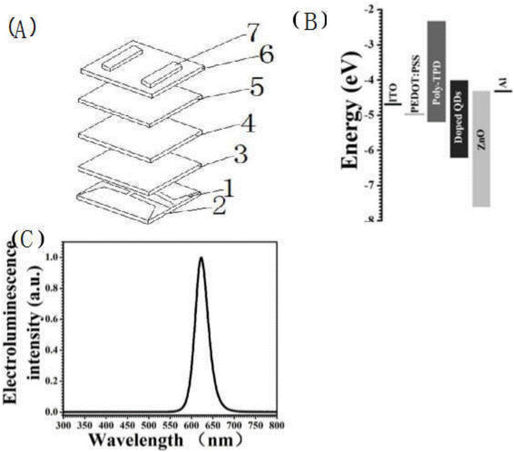
[0035] Take thin film resistor as 20V sq -1 The ITO glass was used as the negative film, and the ITO glass negative film was ultrasonically treated with acetone, absolute ethanol and deionized water for 15 minutes, and then treated with ozone in the air for 5 minutes with a UV lamp. Poly(3,4-ethylenedioxythiophene): polystyrene sulfonate (PEDOT:PSS) was spin-coated on the film, and then baked in air at 150° C. for 15 min. Then spin-coat Poly(9-vinylcarbazole) and bake at 160°C for 30min, CdSe / ZnS quantum dots and the Ga-doped ZnO nanoparticle layer prepared above. The spin-coating rate is 2000rpm, and the spin-coating time of each layer is 60s. Both layers were baked at 70°C for 20 min after spin coating. Then put the prepared multi-layer sample into a customized high-vacuum deposition chamber (the background pressure is about 3×10⁻⁷torr), and deposit the top Ag cathode (100nm thick) to obtain the product.
Embodiment 2
[0037] Prepare Ga-doped ZnO material; the molar ratio of Ga and Zn is 2:100;
[0038] Take thin film resistor as 20V sq -1 The ITO glass was used as the negative film, and the ITO glass negative film was ultrasonically treated with acetone, absolute ethanol and deionized water for 15 minutes, and then treated with ozone in the air for 5 minutes with a UV lamp. Poly(3,4-ethylenedioxythiophene): polystyrene sulfonate (PEDOT:PSS) was spin-coated on the film, and then baked in air at 160° C. for 15 minutes. Then spin-coat Poly(9-vinylcarbazole) and bake at 160°C for 30min, CdSe / ZnS quantum dots and the Ga-doped ZnO nanoparticle layer prepared above. The spin-coating rate is 2000rpm, and the spin-coating time of each layer is 60s. Both layers were baked at 70°C for 20 min after spin coating. Then put the prepared multi-layer sample into a customized high-vacuum deposition chamber (background pressure is about 3×10⁻⁷torr), and deposit the top A1 cathode (100nm thick) to obtain the...
PUM
| Property | Measurement | Unit |
|---|---|---|
| particle diameter | aaaaa | aaaaa |
| thickness | aaaaa | aaaaa |
Abstract
Description
Claims
Application Information