Semiconductor laser with enhanced luminous efficiency

A luminous efficiency and laser technology, applied in the structure of optical resonant cavity, etc., can solve the problem of limited luminous efficiency of semiconductor laser devices, achieve a strong near-field enhancement effect, improve luminous efficiency, and achieve the effect of luminous efficiency

Active Publication Date: 2017-02-15
CHANGCHUN UNIV OF SCI & TECH
View PDF3 Cites 7 Cited by
  • Summary
  • Abstract
  • Description
  • Claims
  • Application Information

AI Technical Summary

Problems solved by technology

These methods can improve the lifetime and reliability of semiconductor laser devices to a certain extent, but have limited effect on improving the luminous efficiency of semiconductor laser devices

Method used


Image

  • Semiconductor laser with enhanced luminous efficiency

Examples


Embodiment Construction

[0008] The technical solutions of the present invention will be described in further detail below with reference to the accompanying drawings and embodiments.

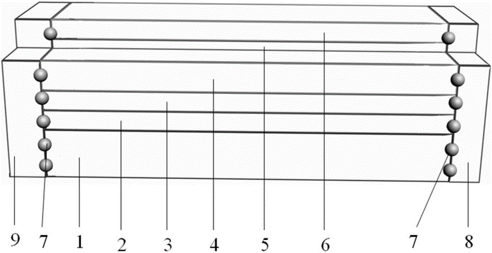
[0009] The invention proposes a semiconductor laser with enhanced luminous efficiency. The semiconductor laser with enhanced luminous efficiency includes a laser chip, metal nanoparticles, an anti-reflection optical film on the front cavity surface of the resonator, and a high-reflection optical film on the rear cavity surface of the resonator. The laser chip structure includes a substrate, a lower confinement layer, a lower waveguide layer, a laser active region, an upper waveguide layer, and an upper confinement layer. The metal nanoparticles are noble metal materials such as Ag, Pt, and Au, and the metal nanoparticles are uniformly distributed in the Diode Laser Resonator Cavity Facets. In the following, the laser chip is a GaAs-based semiconductor laser and Au nanoparticles are taken as an example to describe in de...


PUM


Abstract

The invention discloses a semiconductor laser with enhanced luminous efficiency. According to the laser, on the basis of a traditional semiconductor laser preparation technology, high-vacuum equipment is adopted to performing cleavage on a laser epitaxial wafer in an ultrahigh-vacuum environment and cavity surface metal nanometer particle and cavity surface film preparation are performed. According to the laser disclosed by the invention, uniformly distributed metal nanometer particles are prepared on laser resonance cavity surface, free electrons of metal nanometer particles are utilized to be coupled with incident electromagnetic waves, collective oscillation of free electrons is caused, an enhanced local area electric field is generated, a strong near field enhancing effect is provided, radiative recombination of active region carriers of the laser is enhanced, and improvement of the luminous efficiency of the semiconductor laser device is realized.

Description

technical field [0001] The invention relates to the field of semiconductor lasers, in particular to a semiconductor laser which utilizes metal localized surface plasmons to realize enhanced luminous efficiency. Background technique [0002] Semiconductor lasers have the characteristics of small size, light weight, high reliability, long service life, and low power consumption. They are used in military and civilian fields such as industrial processing, laser medical treatment, laser optical communication, laser ranging, industrial detection, optical storage, and laser printing. Has a wide range of applications. At present, high-quality semiconductor laser chip materials are mostly prepared by epitaxy by molecular beam epitaxy (MBE) and metal organic chemical vapor deposition (MOCVD). Although semiconductor laser material epitaxy technology has made great progress, semiconductor laser devices still have the problem of low luminous efficiency, which seriously limits the impro...

Claims


Application Information

Patent Timeline
Patent Type & Authority Applications(China)
IPC IPC(8): H01S5/10
Inventor 魏志鹏方铉牛守柱唐吉龙王登魁房丹王海珠李金华楚学影马晓辉王晓华
Owner CHANGCHUN UNIV OF SCI & TECH
Why Eureka
Try Eureka