
Eureka
For R&D, Eureka makes reading and utilizing patents & technical documents easy.
Eureka AIR
Designed for self-driven R&D workflows. Generate viable solutions, solve complex R&D challenges, empower your innovation with AI.

Eureka Materials
Designed for material experts only. Revolutionize your material R&D, from search, analyze, to developing new materials.

TechResearch
Generate reliable direction feasibility study reports for your R&D in just a few steps.

TechSeek
Discover and master advanced knowledge NOW. Basics, ideas, possibilities, all at once.

TechMind
As an expert in R&D Theories, TechMind can generates customized viable solutions instantly.

TechRisk
Analyze your overall solution with one click, know your potential R&D risks in advance.

TechMonitor
Get weekly tech updates, stay abreast of the latest tech innovations and key insights.
Developing bath cleaning agent used for manufacture procedure of PCB
A cleaning agent and solvent technology, applied in the field of DES development process, can solve the problems of poor cleaning effect, high COD value, long cleaning time, etc., and achieve the effects of reduced cost, low corrosion and convenient storage.
- Summary
- Abstract
- Description
- Claims
- Application Information
AI Technical Summary
Problems solved by technology
Method used
Image

Examples
Embodiment 1
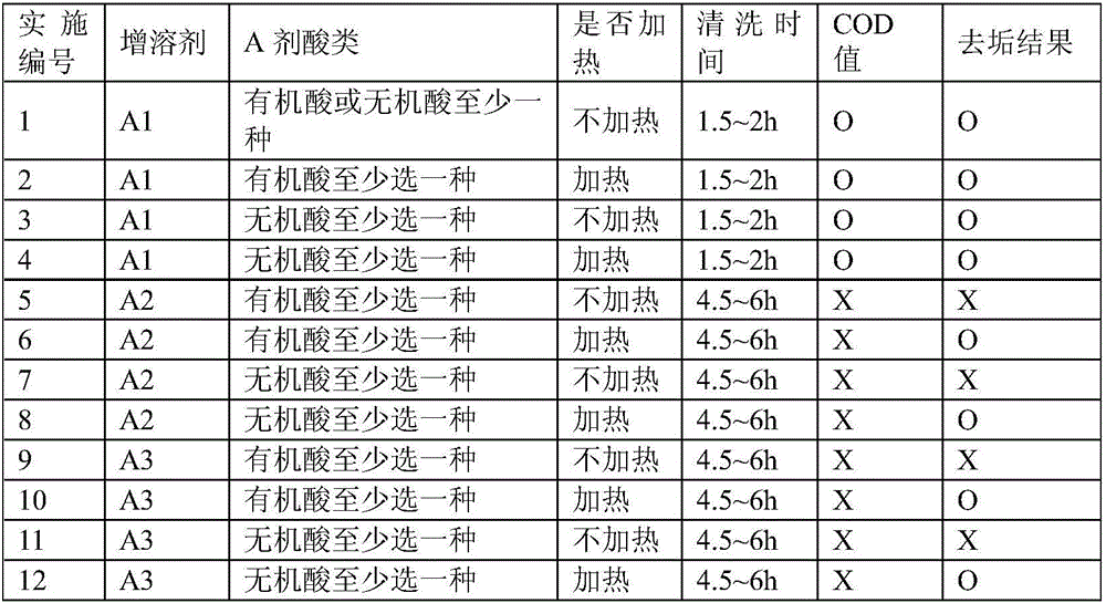
[0022] Solvent A: hydrochloric acid, sulfuric acid, citric acid, phosphoric acid, acetic acid, oxalic acid, formic acid, sulfurous acid, phosphorous acid in any proportion total 100kg, water 900kg.
[0023] Solvent B: based on solvent A, 10kg of polyethylene glycol (accounting for 10 / 1000=1% of the mass of solvent A); 10kg of water-soluble polyether (accounting for 10 / 1000=1% of the mass of solvent A).
[0024] Stir and mix solvent A and solvent B evenly to obtain a slightly light yellow liquid developing tank cleaning agent.
Embodiment 2
[0026] Solvent A: hydrochloric acid, sulfuric acid, citric acid, phosphoric acid, acetic acid, oxalic acid, formic acid, sulfurous acid, phosphorous acid in any proportion total 100kg, water 900kg.
[0027] Solvent B: based on solvent A, polyethylene glycol 20kg (accounting for 20 / 1000=2% of the mass of solvent A); 10kg of water-soluble polyether (accounting for 10 / 1000=1% of the mass of solvent A).
[0028] Stir and mix solvent A and solvent B evenly to obtain a slightly light yellow liquid developing tank cleaning agent.
Embodiment 3
[0030] Solvent A: hydrochloric acid, sulfuric acid, citric acid, phosphoric acid, acetic acid, oxalic acid, formic acid, sulfurous acid, phosphorous acid in any proportion total 100kg, water 900kg.
[0031] Solvent B: based on solvent A, 10kg of polyethylene glycol (accounting for 10 / 1000=1% of the mass of solvent A); 20kg of water-soluble polyether (accounting for 20 / 1000=2% of the mass of solvent A).
[0032] Stir and mix solvent A and solvent B evenly to obtain a slightly light yellow liquid developing tank cleaning agent.
PUM
 Abstract
Description
Claims
Application Information
 - R&D Engineer
- R&D Manager
- IP Professional
- Industry Leading Data Capabilities
- Powerful AI technology
- Patent DNA Extraction
Browse by: Latest US Patents, China's latest patents, Technical Efficacy Thesaurus, Application Domain, Technology Topic, Popular Technical Reports.
© 2024 PatSnap. All rights reserved.Legal|Privacy policy|Modern Slavery Act Transparency Statement|Sitemap|About US| Contact US: help@patsnap.com