Dual-layer perovskite light emitting diode and preparation method therefor

A technology of light-emitting diodes and double-layer perovskites, which is applied in semiconductor/solid-state device manufacturing, electrical components, and electrical solid-state devices, can solve problems such as unfavorable electron transmission, energy waste, and heat loss, and achieve improved luminous efficiency and reduced Turn-on voltage and low processing cost

Active Publication Date: 2017-02-22
SUZHOU UNIV
View PDF3 Cites 37 Cited by
  • Summary
  • Abstract
  • Description
  • Claims
  • Application Information

AI Technical Summary

Problems solved by technology

However, due to the high potential barrier formed between the semiconductor electron transport layer and the perovskite used in the conventional device structure, it is not conducive to the transmission of electrons, and the perovskite light-emitting diode usually has a relatively high turn-on voltage (greater than 3V), so The high turn-on voltage will cause waste of energy and heat loss

Method used


Image

  • Dual-layer perovskite light emitting diode and preparation method therefor
  • Dual-layer perovskite light emitting diode and preparation method therefor
  • Dual-layer perovskite light emitting diode and preparation method therefor

Examples


Embodiment 1

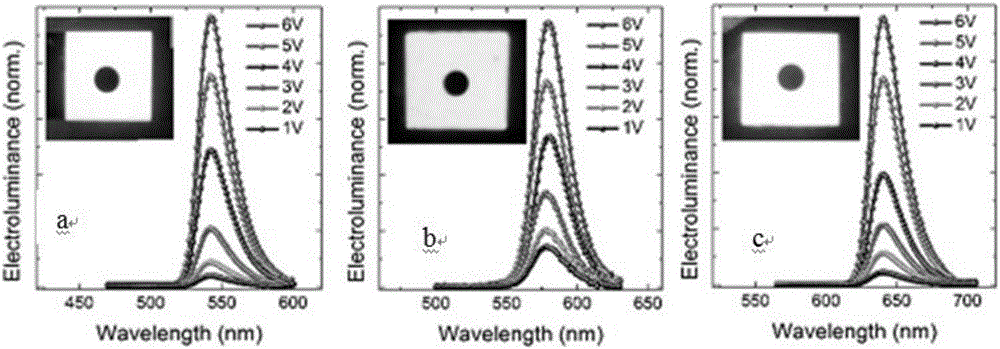
[0042] CH 3 NH 3 PbBr 3 The precursor solution was diluted to a mass ratio of 1.25% to obtain a green light-emitting perovskite solution, and the photoluminescence spectrum of the prepared light-emitting diode was as follows: image 3 as shown in a.

Embodiment 2

[0044] The CH with a mass ratio of 2.5% 3 NH 3 PB 3 and CH at a mass ratio of 1.25% 3 NH 3 PbBr 3 The perovskite precursor solutions of two different systems were mixed according to the molar ratio of 0.3:2.7 to obtain a yellow-emitting perovskite solution. The photoluminescence spectrum of the prepared light-emitting diode was as follows: image 3 As shown in b.

Embodiment 3

[0046] The CH with a mass ratio of 2.5% 3 NH 3 PB 3 and CH at a mass ratio of 1.2% 3 NH 3 PbBr 3 The perovskite precursor solutions of two different systems are mixed according to the molar ratio of 1.05:1.95 to obtain a red-emitting perovskite solution. The photoluminescence spectrum of the prepared light-emitting diode is as follows: image 3 as shown in c.


PUM

PropertyMeasurementUnit
thicknessaaaaaaaaaa
thicknessaaaaaaaaaa

Abstract

The invention relates to a dual-layer perovskite light emitting diode and a preparation method therefor. The dual-layer perovskite light emitting diode comprises the following components from the bottom up separately: ITO conductive glass is used as a positive electrode; a layer of poly 3, 4-ethylenedioxythiophene-polystyrolsulfon acid (PEDOT-PSS) with a thickness of about 20nm is used as a hole transport layer; a dual-layer perovskite light emitting layer is prepared by a spin-coating method in two times; the adopted dual-layer perovskite light emitting layer can be perovskite with different halogen ratios; a layer of calcium-doped zinc oxide (Ca:ZnO) with the thickness of about 50nm is spin-coated on the perovskite layer to be used as an electron transport layer; and finally metal calcium and aluminum are evaporated to be used as a negative electrode. According to the dual-layer perovskite light emitting diode and the preparation method therefor, on one hand, by regulating and controlling the Ca concentration in the Ca:ZnO, an optimal band gap is obtained, so that the barrier between the electron transport layer and the perovskite is reduced, and the cut-in voltage of the light emitting diode is lowered consequently, and the light emitting efficiency and internal quantum efficiency of the light emitting diode are improved at the same time; and on the other hand, by regulating the halogen ratios in the perovskite, light emission with different colors can be realized.

Description

technical field [0001] The invention belongs to the field of electroluminescent devices, in particular to a double-layer perovskite light-emitting diode and a preparation method thereof. Background technique [0002] Metal halide perovskite materials can be expressed by the chemical formula MAPbX 3 to represent, where X is Br, I, and / or Cl, this type of material has excellent photoelectric properties and can be applied to photoelectric devices such as solar cells, photodetectors, and light-emitting diodes. Perovskite-based light-emitting diodes have the characteristics of high luminous purity, high emission efficiency and low excitation energy, so they may become new light-emitting materials that replace inorganic quantum dots and traditional organic light-emitting materials. However, due to the high potential barrier formed between the semiconductor electron transport layer and the perovskite used in the conventional device structure, it is not conducive to the transmissio...

Claims


Application Information

Patent Timeline
Patent Type & Authority Applications(China)
IPC IPC(8): H01L51/50H01L51/52H01L51/56
CPCH10K50/00H10K50/11H10K50/80H10K50/805H10K71/00
Inventor 鲍桥梁卡西木李绍娟李鹏飞
Owner SUZHOU UNIV
Why Eureka
Try Eureka