Printing plate, method for producing printing plate, method for manufacturing functional element and printing apparatus
A manufacturing method and technology for printing plates, applied in the preparation of printing surfaces, printing devices, printing and other directions, can solve problems such as electrical short circuit, plate contamination, resolution reduction, etc. dirty effect
- Summary
- Abstract
- Description
- Claims
- Application Information
AI Technical Summary
Problems solved by technology
Method used
Image
Examples
Embodiment 1
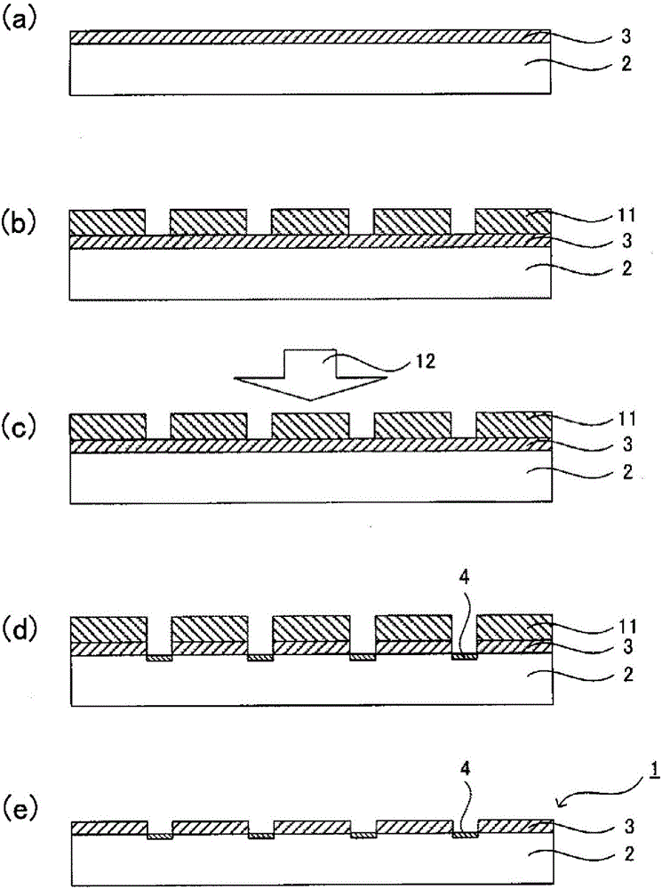
[0281] [Example 1] Production of a lithographic printing plate utilizing silicone rubber
[0282] (Making of base material)
[0283] Shin-Etsu Silicone KE106 manufactured by Shin-Etsu Chemical Co., Ltd., which is a stock solution of silicone rubber, was spin-coated on a glass substrate using a spin coater MS-A100 manufactured by Mikasa Co., Ltd., and a hot plate ND-1 manufactured by AS ONE Co., Ltd. It heated at 160 degreeC for 1 hour, and the silicone rubber layer was formed. The contact angle of the silicone rubber layer with respect to pure water was measured with a contact angle meter DM-901 manufactured by Kyowa Interface Science Co., Ltd. and found to be 107±4°. In addition, when the thickness of the silicone rubber layer was measured using a standard digital caliper (Digimatic Calipers) manufactured by Mitutoyo Corporation, it was 620 μm.
[0284] The surface of the silicone rubber layer was subjected to oxygen plasma treatment using a plasma cleaner V1000 manufacture...
Embodiment 2
[0291] [Example 2] Production of a printing plate for gravure printing using silicone rubber
[0292] (Preparation of substrate and formation of hydrophobic solvent permeation prevention layer)
[0293] A substrate was produced in the same manner as in Example 1 to form a hydrophobic solvent permeation preventing layer.
[0294] (patterning of version)
[0295] In the same manner as in Example 1, a resist pattern was formed on the surface of the hydrophobic solvent penetration preventing layer.
[0296] Using the plasma cleaner V1000 manufactured by Yamato Scientific Co., Ltd., the hydrophobic solvent permeation prevention layer and the silicone rubber layer formed with the resist pattern are treated with oxygen and CF. 4 After the plasma generated by the mixed gas is treated, the oxygen plasma treatment is directly performed without opening in batches. At this time, in the opening of the resist pattern, the hydrophobic solvent permeation prevention layer is removed by perf...
Embodiment 3
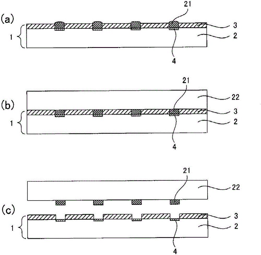
[0301] [Example 3] Preparation of an electrode for an organic thin film transistor (OTFT, Organic Thin Film Transistor)
[0302] (production of print edition)
[0303] A printing plate for lithographic printing was produced in the same manner as in Example 1 except that a photomask having a pattern corresponding to a source electrode and a drain electrode of an OTFT was used. On the surface of the plate, regions corresponding to source electrodes and drain electrodes are hydrophobic regions, and other regions are hydrophilic regions.
[0304] (Making of blanket layer)
[0305] The surface of polyethylene naphthalate (PEN, PolyethyleneNaphthalate) film Q65FA manufactured by Teijin Dupont Co., Ltd. was cleaned by vacuum ultraviolet light treatment using a light irradiation device UER616908-172 manufactured by Ushio Electric Corporation. Next, uncured silicone rubber KE106 manufactured by Shin-Etsu Silicones was spin-coated on the PEN film using a spin coater MS-300 manufacture...
PUM
| Property | Measurement | Unit |
|---|---|---|
| width | aaaaa | aaaaa |
| thickness | aaaaa | aaaaa |
| thickness | aaaaa | aaaaa |
Abstract
Description
Claims
Application Information
 - R&D
- Intellectual Property
- Life Sciences
- Materials
- Tech Scout
- Unparalleled Data Quality
- Higher Quality Content
- 60% Fewer Hallucinations
Browse by: Latest US Patents, China's latest patents, Technical Efficacy Thesaurus, Application Domain, Technology Topic, Popular Technical Reports.
© 2025 PatSnap. All rights reserved.Legal|Privacy policy|Modern Slavery Act Transparency Statement|Sitemap|About US| Contact US: help@patsnap.com


