

Preparation method of silicon wafer/poly-2-vinylpyridine brush/polypyrrole-gold nanoparticle composite material
A technology of vinylpyridine brush and vinylpyridine, which is applied in the field of conductive polymer noble metal composite materials, can solve the problems of limited and enhanced Raman signal ability, and achieve the effect of strong SERS activity
- Summary
- Abstract
- Description
- Claims
- Application Information
AI Technical Summary
Problems solved by technology
Method used
Image

Examples
Embodiment 1
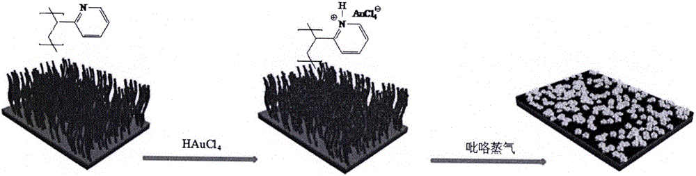
[0028] Step 1: Dip the silicon wafer coated with silicon dioxide on the surface into a toluene solution (10 wt%) containing 3-aminopropyltriethoxysilane, and ultrasonicate for 30 minutes to form amino groups on the surface of the silicon wafer. Subsequently, the amino-modified silicon wafer was immersed in a sealed tube containing 2-vinylpyridine monomer, and irradiated with ultraviolet light (wavelength 350nm) for 1.5 hours at room temperature. P2VP polymers branched onto silicon wafers, yielding silicon wafer / P2VP brushes.
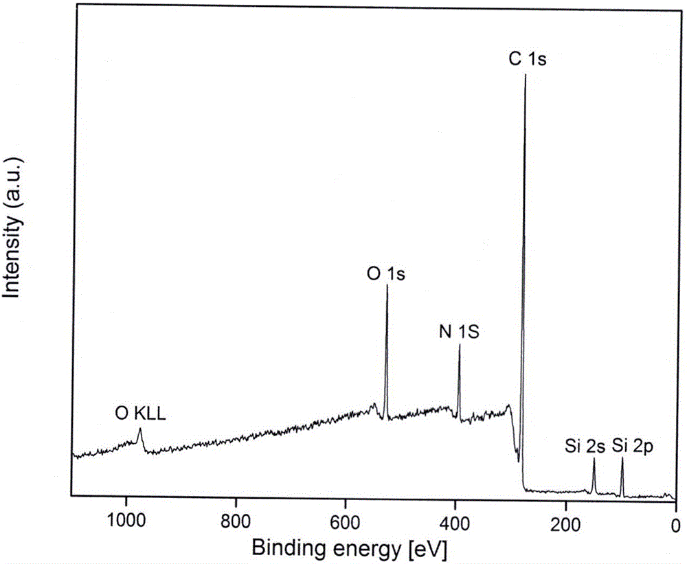
[0029] figure 2 It is the XPS diagram of the silicon wafer / P2VP brush. In the figure, 01s, Si2s, and Si2p belong to the silicon dioxide layer on the silicon wafer, and C1s and N1s belong to the P2VP; thus proving that the P2VP polymer brush has been successfully grafted to the silicon wafer surface .
[0030] Step 2: Soak the silicon wafer / P2VP brush obtained in step 1 in an aqueous solution of chloroauric acid (1% wt) for 12 hours, then take it out a...
Embodiment 2
[0034] Step 1: Use Step 1 of Embodiment 1 to obtain a silicon wafer / P2VP brush.
[0035]Step 2: Soak the silicon wafer / P2VP brush obtained in step 1 in an aqueous solution of chloroauric acid (1% wt) for 12 hours, then take it out and wash it with deionized water to remove unadsorbed chloroauric acid. Subsequently, the adsorbed AuCl 4 - The ionic P2VP brush is placed in a closed container containing pyrrole solution, and the poly 2-vinylpyridine brush is not in contact with pyrrole, and the pyrrole vapor formed by volatilization of the pyrrole solution is combined with the AuCl in the P2VP brush. 4 - Ion reaction, controlled reaction time 120min, pyrrole vapor was AuCl 4 Oxidative polymerization into polypyrrole, while AuCl 4 - The ions themselves are reduced to flower-like Au nanostructures.
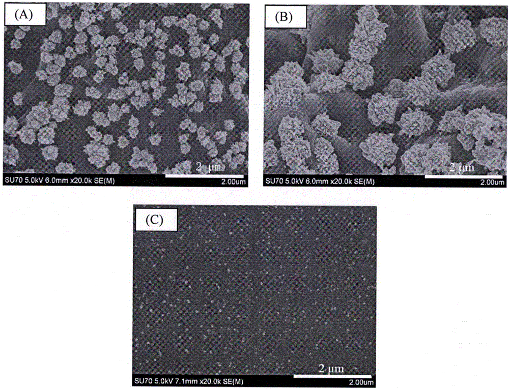
[0036] image 3 (B) is the SEM image of the obtained silicon wafer / P2VP brush / PPy-Au composite material, and Au nanostructures with flower-like structure are obtained.
reference example 1
[0042] P2VP brush / PPy-Au composite as Raman substrate for detection of 4-aminothiophenol (4-ATP)
[0043] Previous theories have proved that noble metal nanostructures with complex structures can provide "hot spots" for Raman enhancement. We chose 4-aminothiophenol (4-ATP) as an example of small organic molecules to test its surface-enhanced Raman active. We chose the silicon wafer / P2VP brush / PPy-Au composite material prepared in Example 1 as the base material for the Raman test. First prepare a concentration of 1×10 -4 M in 4-ATP ethanol solution, then soak the silicon wafer / P2VP brush / PPy-Au composite into the 4-ATP solution, take it out after 6 hours, wash it with pure ethanol for 3 times, and finally dry it with a high-purity nitrogen stream , for Raman testing. Figure 5 It is the SERS spectrum of silicon wafer / P2VP brush / PPy-Au composite material and the Raman spectrum of pure solid 4-ATP, where the Raman spectrum of 4-ATP is amplified by 5 times.
[0044] From Fig...
PUM
| Property | Measurement | Unit |
|---|---|---|
| wavelength | aaaaa | aaaaa |
Abstract
Description
Claims
Application Information