Method of manufacturing flexible stress sensor based on nano conductive material

A stress sensor and nano-conducting technology, applied in the field of biosensors, to achieve the effects of good stretchability, high sensitivity, improved sensitivity and stretchability

Active Publication Date: 2017-03-15
TAIYUAN UNIV OF TECH
View PDF6 Cites 32 Cited by
  • Summary
  • Abstract
  • Description
  • Claims
  • Application Information

AI Technical Summary

Problems solved by technology

In this preparation method, a certain-sized sheet is used as a template to prepare a grooved PDMS film, which solves many problems in the preparation process of the existing flexible stress sensor based on nano-conductive materials.

Method used


Image

  • Method of manufacturing flexible stress sensor based on nano conductive material

Examples


preparation example Construction

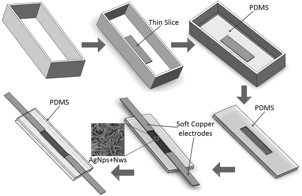
[0018] A method for preparing a flexible stress sensor based on conductive nanomaterials, comprising the steps of:

[0019] 1) Take a flat-bottomed container and place a sheet in the center of the flat-bottomed container;

[0020] 2) Prepare the PDMS solution, take the main agent and the curing agent at a mass ratio of 10:1, put it in a petri dish and mix evenly, and use a vacuum drying oven to evacuate for 10 minutes to break the bubbles in the mixed solution to obtain a PDMS solution without bubbles on the surface;

[0021] 3) Add the PDMS solution prepared in step 2) into the flat-bottomed container prepared in step 1), so that the PDMS solution covers the sheet;

[0022] 4) Put the flat-bottomed container containing PDMS and flakes into 70 o Heating in the drying oven of C for 1.5h, the PDMS solution forms a PDMS film;

[0023] 5) Take out the PDMS film in the flat-bottomed container, remove the sheet, and obtain a PDMS flexible template with grooves;

[0024] 6) After ...

Embodiment 1

[0031] 1) Take a 2*1cm rectangular low-wall flat-bottomed container, and put a 0.8*0.3*0.05cm silicon wafer in the center;

[0032] 2) Prepare the PDMS solution, take the main agent and the curing agent at a mass ratio of 10:1, put it in a petri dish and mix evenly, and use a vacuum drying oven to evacuate for 10 minutes to break the bubbles in the mixed solution to obtain a PDMS solution without bubbles on the surface;

[0033] 3) Take the PDMS solution prepared in step 2) and add it to the container prepared in step 1);

[0034] 4) Put the container with PDMS and silicon wafer into 70 o Heating in a drying oven at C for 1.5h;

[0035] 5) Take out the PDMS film in the container, remove the silicon wafer, and obtain a PDMS flexible template with grooves;

[0036] 6) After drawing out the electrodes with conductive copper tape on the two narrow sides of the groove, fill the groove with silver nanowires, a nano-conductive material;

[0037] 7) After the sol is completely dry,...

Embodiment 2

[0039] A core-shell structure conductive polyaniline / Co 3 o 4 The preparation method of powder, comprises the steps:

[0040] 1) Take a circular container with a short wall and a flat bottom with a diameter of 2 cm, and place a silicon wafer with a diameter of 0.8 cm and a thickness of 0.05 cm in the center;

[0041] 2) Prepare the PDMS solution, take the main agent and the curing agent at a mass ratio of 10:1, put it in a petri dish and mix evenly, and use a vacuum drying oven to evacuate for 10 minutes to break the bubbles in the mixed solution to obtain a PDMS solution without bubbles on the surface;

[0042] 3) Take the PDMS solution prepared in step 2) and add it to the container prepared in step 1);

[0043] 4) Put the container with PDMS and silicon wafer into 70 o Heating in a drying oven at C for 1.5h;

[0044] 5) Take out the PDMS film in the container, remove the silicon wafer, and obtain a PDMS flexible template with grooves;

[0045] 6) After the electrodes are...


PUM

PropertyMeasurementUnit
diameteraaaaaaaaaa
diameteraaaaaaaaaa
thicknessaaaaaaaaaa

Abstract

The invention discloses a method of manufacturing a flexible micro membrane surface stress biosensor based on a nano conductive material. Particularly, a simple method is used for combining the nano conductive material and a flexible substrate, and the sensitivity and the telescopic performance of the stress sensor are further improved. Firstly, a flexible material (such as PDMS) is used as a raw material to make a flexible template with a groove; then, the nano conductive material (such as carbon nanotubes or silver nanowires) is used for filling the groove in the template; electrodes are led out from two ends of the filled nano conductive material; and finally, a flexible polymer material (such as PDMS) is used for fixing the nano material and the electrodes at the upper layer, and the structure stability is enhanced (the step can be omitted according to actual demands). The method of the invention has the advantages that the process is simple; the cost is low; the controllability is strong; the manufactured flexible stress sensor based on the nano conductive material is high in sensitivity, high in stability and good in flexibility; and possibilities are provided for realizing miniaturization, low cost and batch production.

Description

technical field [0001] The invention relates to the field of biosensors, in particular to a method for preparing a flexible microfilm stress sensor based on conductive nanomaterials. Background technique [0002] Flexible wearable electronic devices have received more and more attention due to their convenient interaction with the human body. Flexible and stretchable wearable sensors can be easily mounted on clothing or directly attached to the body to realize human motion and temperature change detection with high stretchability and sensitivity. [0003] PDMS, also known as organosilicon, is a high molecular organosilicon compound. The cured PDMS is a kind of silica gel, which has many characteristics, such as transparency, non-toxicity, hydrophobicity, non-flammability, easy bonding with various materials at room temperature, etc., and has good elasticity due to its low Young's modulus . At the same time, PDMS has very good temperature resistance, and its maximum temper...

Claims


Application Information

Patent Timeline
Patent Type & Authority Applications(China)
IPC IPC(8): G01L1/20
CPCG01L1/20
Inventor 张强桑胜波菅傲群段倩倩冀建龙张文栋刘丽华赵冬
Owner TAIYUAN UNIV OF TECH
Why Eureka
Try Eureka