Method for reducing the polysilicon surface roughness

A surface roughness and polysilicon technology, which is applied in the manufacture of electrical components, electrical solid devices, semiconductor/solid devices, etc., can solve the problems of large leakage current of TFT, high surface roughness of polysilicon film, easy formation of parasitic capacitance, etc.

Inactive Publication Date: 2017-04-26
WUHAN CHINA STAR OPTOELECTRONICS TECH CO LTD
View PDF4 Cites 1 Cited by
  • Summary
  • Abstract
  • Description
  • Claims
  • Application Information

AI Technical Summary

Problems solved by technology

[0010] The purpose of the present invention is to solve the problem that the surface roughness of the polysilicon film obtained by the existing LTPS production process is

Method used


Image

  • Method for reducing the polysilicon surface roughness
  • Method for reducing the polysilicon surface roughness
  • Method for reducing the polysilicon surface roughness

Examples


Embodiment 1

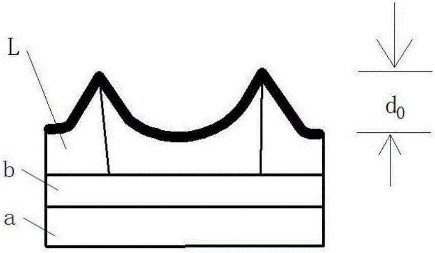
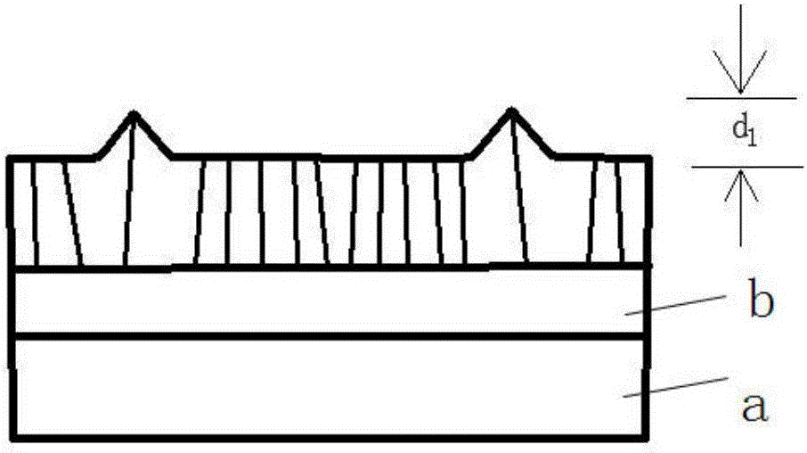
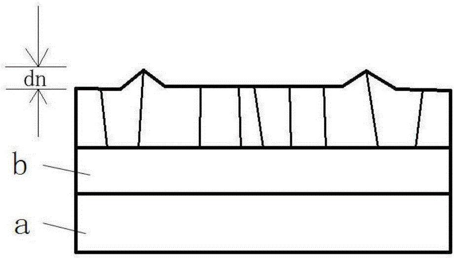
[0057] The method for reducing the surface roughness of polysilicon in this embodiment comprises the following steps:

[0058] 1. Use O with a concentration of 5mg / L 3 Water contacts the surface of the polysilicon layer for oxidation treatment for 15 seconds, thereby forming a surface oxide layer;

[0059] 2. Contacting the surface oxide layer formed on the surface of the polysilicon layer with an HF solution with a concentration of 1 wt% for 40 seconds to obtain an oxidized and etched polysilicon layer;

[0060] 3. Repeat the oxidation treatment of step 1 and the etching treatment of step 2 three times in sequence, thereby reducing the surface roughness of the polysilicon.

[0061] This embodiment controls O 3 The concentration of water is low, so that the thickness of the oxide layer on the surface after each oxidation treatment is also thinner. Subsequently, the polysilicon with the oxide layer on the surface is etched with a HF solution with a lower concentration. Due to...

Embodiment 2

[0064] The method for reducing the surface roughness of polysilicon in this embodiment is realized in the following steps:

[0065] 1. The buffer layer and the amorphous silicon layer are sequentially deposited on the glass substrate by PECVD method;

[0066] 2. Heat the amorphous silicon layer described in step 1 at 500° C. for 1.5 hours, and then carry out an excimer laser annealing treatment to the amorphous silicon layer to form a polysilicon layer;

[0067] 3. Use O with a concentration of 10mg / L 3 Water is contacted with the surface of the polysilicon layer formed in step 2 for oxidation treatment for 15 seconds, thereby forming a surface oxide layer;

[0068]4. Contact the surface oxide layer formed on the surface of the polysilicon layer with a concentration of 2wt% HF solution for etching for 50 seconds to obtain a polysilicon layer that has been oxidized and etched;

[0069] Fifth, repeating the oxidation treatment of step three and the etching treatment process of...


PUM

PropertyMeasurementUnit
Thicknessaaaaaaaaaa
Thicknessaaaaaaaaaa

Abstract

The invention relates to a method for reducing the polysilicon surface roughness, comprising the following steps: i) letting O3 water contact the surface of a polysilicon layer for an oxidation process; forming a surface oxidation layer on the surface of the polysilicon layer; ii) letting the surface oxidation layer formed on the surface of the polysilicon layer contact HF solution for an etching process to obtain a polysilicon layer after the oxidation process and the etching process; iii) repeating the oxidation process of step i) and the etching process of step ii) for n times until the height of the bump at the polysilicon interface is less than 30 nm, where n is a positive integer. The method of the invention utilizes O3 water to oxidize the surface of the polysilicon layer. Since O3 has a strong oxidizing property, the oxidation time can be shortened greatly; and then after plural times of oxidation processes and etching processes, the surface flatness of the polysilicon film is greatly improved in order to reduce the leakage current of a thin film transistor and optimize the electric properties thereof.

Description

technical field [0001] The invention belongs to the technical field of liquid crystal panel manufacture, and in particular relates to a method for reducing the surface roughness of polysilicon in thin film transistors. Background technique [0002] A thin film transistor (TFT) of a liquid crystal display element is composed of a silicon film formed on an insulating substrate, and is used as a switching element provided in a pixel of a liquid crystal display element or a driving element formed in a peripheral circuit portion. As a silicon film constituting a TFT, an amorphous silicon film is mostly used, but in recent years, a polysilicon film having better characteristics has been increasingly used, and much development work is currently being carried out in this regard. The formation of polysilicon film needs to be carried out at high temperature, but because the heat resistance of the insulating substrate is low, it is easy to cause substrate deformation. Therefore, low te...

Claims


Application Information

Patent Timeline
IPC IPC(8): H01L21/02H01L21/311H01L21/306H01L27/12
CPCH01L21/02164H01L21/02238H01L21/30604H01L21/31111H01L27/127
Inventor 李勇
Owner WUHAN CHINA STAR OPTOELECTRONICS TECH CO LTD
Why Eureka
Try Eureka