Ultra broadband spectrum light-sensitive material and photoelectric detector employing same

A technology of photodetectors and photosensitive materials, applied in the field of optoelectronics, can solve the problems of increasing equipment costs, complex and even huge systems, and achieve the effects of convenient production, wide range of spectral detection, and wide range of applicable temperature ranges

Inactive Publication Date: 2017-04-26
SUN YAT SEN UNIV
View PDF8 Cites 5 Cited by
  • Summary
  • Abstract
  • Description
  • Claims
  • Application Information

AI Technical Summary

Problems solved by technology

These harsh refrigeration conditions greatly increase the cost of equipment, making the system complex and even large, causing a lot of inconvenience during use

Method used


Image

  • Ultra broadband spectrum light-sensitive material and photoelectric detector employing same
  • Ultra broadband spectrum light-sensitive material and photoelectric detector employing same
  • Ultra broadband spectrum light-sensitive material and photoelectric detector employing same

Examples


Embodiment 1

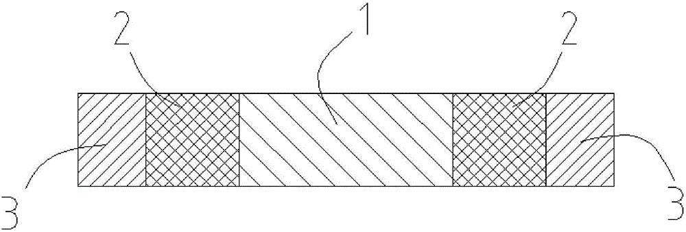
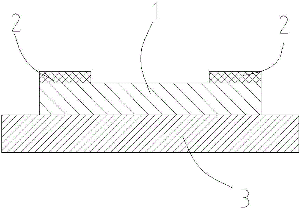
[0047] This embodiment discloses a photodetector, such as Figure 1~2 As shown, it includes a single photosensitive unit 1, the shape of the photosensitive unit 1 is a cuboid, and the insulating substrate 3 arranged under the photosensitive unit 1 is a sapphire sheet with a thickness of 1 mm.

[0048] In this embodiment, the photosensitive area of ​​the photosensitive unit 1 is specifically 0.9mm×0.18mm.

[0049] In this embodiment, the preparation material of the photosensitive unit 1 is specifically EuSb 0.8 Te 3.2 Ternary telluride crystals.

[0050] In this embodiment, the metal electrodes 2 are specifically two gold electrodes, and the two are respectively deposited on both ends of the photosensitive unit 1 through a coating process.

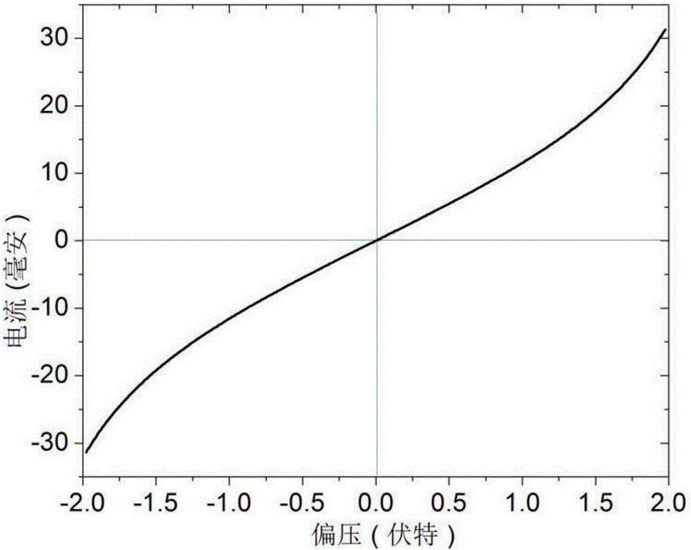
[0051] The inventor tests the photodetector described in this embodiment, and the results are as follows:

[0052] (1) The characteristic current-voltage (I-V) curve that the photodetector described in the present embodiment measures un...

Embodiment 2

[0055] This embodiment discloses another photodetector, such as Figure 1~2 , similarly, it only includes a single photosensitive unit 1, the shape of the photosensitive unit 1 is a cuboid, and the insulating substrate 3 arranged under the photosensitive unit 1 is a sapphire sheet with a thickness of 1mm.

[0056] In this embodiment, the photosensitive area of ​​the photosensitive unit 1 is specifically 0.85mm×0.22mm.

[0057] In this embodiment, the preparation material of the photosensitive unit 1 is specifically EuBi 0.75 Te 3.2 Ternary telluride crystals.

[0058] In this embodiment, the metal electrodes 2 are specifically two gold electrodes, and the two are respectively deposited on both ends of the photosensitive unit 1 through a coating process.

[0059] The inventor tests the photodetector described in this embodiment, and the results are as follows:

[0060] (1) The characteristic current-voltage (I-V) curve that the photodetector described in the present embodim...


PUM

PropertyMeasurementUnit
thicknessaaaaaaaaaa

Abstract

The invention discloses an ultra broadband spectrum light-sensitive material, and the material contains Eu-Sb-Te ternary telluride crystals or Eu-Bi-Te ternary telluride crystals. The invention also discloses a photoelectric detector employing the material, and the detector comprises a light sensing unit which can carry out photoelectric conversion. Two ends of the light sensing unit are respectively provided with a metal electrode, and the material of the light sensing unit contains the former ultra broadband spectrum light-sensitive material. According to the invention, the ultra broadband spectrum light-sensitive can achieve the photoelectric conversion in the ranges of ultraviolet, visible, infrared and terahertz bands, and is wide in application range of temperature. The photoelectric detector can achieve the light detection in the ranges of ultraviolet, visible, infrared and terahertz bands, and the working temperature section is from 77K to 400K. In addition, the photoelectric detector is simple in structure, facilitates large-scale integration through combining with the crystal growth technology and the film preparation technology, is convenient to make, and remarkably reduces the preparation cost under the condition that the performance of the detector is effectively improved.

Description

technical field [0001] The invention belongs to the technical field of optoelectronics, and in particular relates to an ultra-wide spectrum photosensitive material and a photodetector using the photosensitive material. Background technique [0002] At present, photodetectors, as the core equipment in various optoelectronic systems, have been widely used in communication, remote sensing, security, spectral analysis, biomedicine, space exploration and other fields. However, there are still great difficulties in the use of traditional photodetectors in room temperature terahertz (0.1-10THz) detection technology and multi-channel photodetection technology with ultra-wide spectrum up to terahertz. The main reason is the lack of Photosensitive materials that are sensitive to ultra-broad spectrum including terahertz light at room temperature. [0003] For example, the energy of terahertz photons is small, on the order of millielectronvolts (meV), while the energy gaps of tradition...

Claims


Application Information

Patent Timeline
Patent Type & Authority Applications(China)
IPC IPC(8): H01L31/0272H01L31/0328H01L31/08C01B19/00
CPCH01L31/0272H01L31/0328H01L31/085C01B19/007
Inventor 吴东牛营营
Owner SUN YAT SEN UNIV
Why Eureka
Try Eureka