Forming method of semiconductor structure

A technology of semiconductor and gate structure, applied in the field of formation of semiconductor structure, can solve the problem that the electrical performance of the semiconductor structure needs to be improved, etc.

Active Publication Date: 2017-05-10
SEMICON MFG INT (SHANGHAI) CORP +1
View PDF1 Cites 11 Cited by
  • Summary
  • Abstract
  • Description
  • Claims
  • Application Information

AI Technical Summary

Problems solved by technology

[0004] Although the introduction of high-k metal gates can improve the electrical properties of semiconductor structures to a certain extent, the electrical properties of semiconductor structures formed by existing technologies still need to be improved.

Method used


Image

  • Forming method of semiconductor structure
  • Forming method of semiconductor structure
  • Forming method of semiconductor structure

Examples


Embodiment Construction

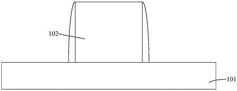
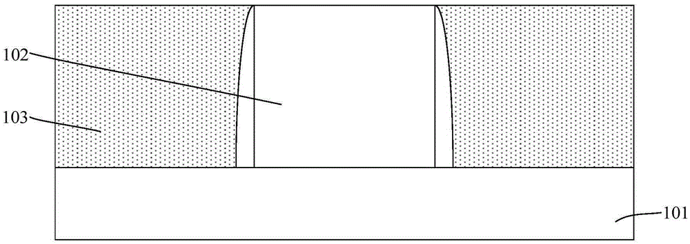
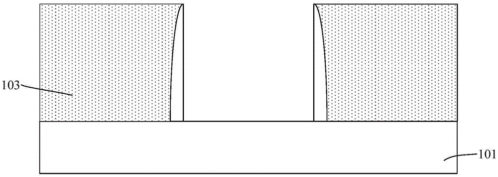
[0031] As mentioned in the background art, the electrical performance of the semiconductor structure formed in the prior art needs to be improved.

[0032] It has been found through research that although the use of a high-k gate dielectric material as the material of the gate dielectric layer can improve the electrical performance of the semiconductor structure to a certain extent, for example, the leakage current (leakagecurrent) in the semiconductor structure is reduced, however, the semiconductor structure The relaxation current (DR Current, DielectricRelaxation Current) is still large, resulting in poor electrical performance of the semiconductor structure, for example, the positive bias-temperature instability characteristics (PBTI, Positive Biase Temperature Instability) and negative bias-temperature instability of the semiconductor structure The stability characteristic (NBTI, Negative Biase Temperature Instability) is remarkable. Further studies have found that the re...


PUM

PropertyMeasurementUnit
thicknessaaaaaaaaaa
thicknessaaaaaaaaaa

Abstract

A forming method of a semiconductor structure includes the following steps: providing a substrate; forming a high k gate medium layer on the surface of the substrate; forming a sacrificial layer on the surface of the high k gate medium layer; conducting defect passivation annealing on the high k gate medium layer, wherein the defect passivation annealing is carried out in an atmosphere lacking defect passivation ions, and the defect passivation ions enter the high k gate medium layer via the sacrificial layer during the defect passivation annealing process; removing the sacrificial layer; and forming a gate electrode layer on the surface of the high k gate medium layer. According to the method, a problem of dielectric relaxation of the high k gate medium layer is overcome, the density of the high k gate medium layer and the density of an interfacial layer are increased, and thus the electrical performance of a semiconductor structure formed by the method is improved.

Description

technical field [0001] The invention relates to the technical field of semiconductor manufacturing, in particular to a method for forming a semiconductor structure. Background technique [0002] The main semiconductor device of an integrated circuit, especially a very large scale integrated circuit, is a metal-oxide-semiconductor field effect transistor (MOS transistor). With the continuous development of integrated circuit manufacturing technology, the technology nodes of semiconductor devices are continuously reduced, and the geometric dimensions of semiconductor structures are continuously reduced following Moore's law. When the size of the semiconductor structure is reduced to a certain extent, various secondary effects caused by the physical limit of the semiconductor structure appear one after another, and it becomes more and more difficult to scale down the feature size of the semiconductor structure. Among them, in the field of semiconductor manufacturing, the most ...

Claims


Application Information

Patent Timeline
Patent Type & Authority Applications(China)
IPC IPC(8): H01L21/336H01L21/28H01L29/40
CPCH01L29/408H01L29/42364H01L29/66477H01L21/28008
Inventor 李勇
Owner SEMICON MFG INT (SHANGHAI) CORP
Why Eureka
Try Eureka