Memristor and application thereof

A memristor and top electrode technology, applied in the field of microelectronics, can solve the problems of material microstructure changes, difficulty in ensuring the cyclic stability and anti-fatigue characteristics of synaptic devices, and achieve good plasticity, enhanced time retention and anti-fatigue. performance, reducing power consumption

Active Publication Date: 2017-05-10
NINGBO INST OF MATERIALS TECH & ENG CHINESE ACADEMY OF SCI
View PDF4 Cites 25 Cited by
  • Summary
  • Abstract
  • Description
  • Claims
  • Application Information

AI Technical Summary

Problems solved by technology

However, a large operating voltage will inevitably lead to changes in the microstructure of the mater...

Method used


Image

  • Memristor and application thereof
  • Memristor and application thereof
  • Memristor and application thereof

Examples


Embodiment 1

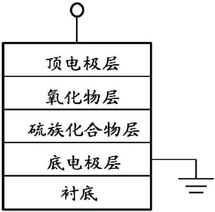
[0036] A memristor comprises sequentially forming a bottom electrode layer, an intermediate dielectric layer and a top electrode layer on a substrate, and the intermediate dielectric layer is composed of a chalcogenide compound layer and an oxide layer. The substrate of this embodiment is a thermally oxidized silicon wafer, and the bottom electrode layer material is platinum; the chalcogenide layer material is ZnS, and its thickness is 70nm; the oxide layer material is ZnO, and its thickness is 20nm; , with a thickness of 50 nm.

[0037] The preparation method of the memristor of the present embodiment is as follows:

[0038](1) A 20nm-thick titanium film was prepared on the surface of the substrate by electron beam evaporation as a buffer layer. The main function is to increase the mechanical bonding force between the platinum film and the thermally oxidized silicon wafer and prevent the film from falling off.

[0039] The aforementioned substrate is a thermally oxidized sil...

Embodiment 2

[0054] The difference from Example 1 is that in the intermediate dielectric layer, the thickness of zinc sulfide is 30nm, and the thickness of zinc oxide is 10nm.

Embodiment 3

[0056] The difference from Example 1 is that the thickness of the intermediate dielectric layer zinc sulfide is 50nm, and the thickness of zinc oxide is 20nm.


PUM

PropertyMeasurementUnit
Thicknessaaaaaaaaaa
Thicknessaaaaaaaaaa
Thicknessaaaaaaaaaa

Abstract

The invention provides a memristor, which comprises a bottom electrode layer, an intermediate medium layer and a top electrode layer which are sequentially formed on a substrate, wherein the intermediate medium layer comprises a chalcogenide layer and an oxide layer; the chalcogenide layer is connected with the bottom electrode layer; and the oxide layer is connected with the top electrode layer. A proper top electrode is adopted to be combined with the oxide layer and the chalcogenide layer, so that the prepared memristor has ultralow operating voltage and has ultrahigh electric sensitivity. The invention further provides an application of the memristor in preparation of a neural synaptic bionic device. The memristor has good synaptic plasticity and achieves short-range plasticity and long-range plasticity under the ultralow operating voltage; and the neural synaptic bionic device with high sensitivity is successfully prepared.

Description

technical field [0001] The invention relates to the technical field of microelectronics, in particular to a memristor and its application. Background technique [0002] Memristor (memristor) is the fourth basic passive electronic device besides resistors, capacitors, and inductors. "Cai Shaotang" first deduced the existence of this element when studying the relationship between charge, current, voltage and magnetic flux in the 1970s, and pointed out that it represented the relationship between charge and magnetic flux. Memristors have the dimension of resistance, but have nonlinear electrical properties different from ordinary resistors. A memristor's resistance changes in response to the amount of charge flowing through it, and it maintains its resistance when the current is turned off. The resistance value of this current-controlled memristive system satisfies a certain mathematical relationship with the applied voltage and time. However, an ideal device with this mathem...

Claims


Application Information

Patent Timeline
IPC IPC(8): H01L45/00
CPCH10N70/245H10N70/882H10N70/883
Inventor 诸葛飞胡令祥曹鸿涛
Owner NINGBO INST OF MATERIALS TECH & ENG CHINESE ACADEMY OF SCI
Why Eureka
Try Eureka