Femtosecond laser direct writing preparation method of two-dimensional submicron butterfly-shaped metal microstructure

A technology of metal microstructure and femtosecond laser, which is applied in laser welding equipment, metal processing equipment, welding equipment, etc., can solve the problems of multiple procedures and complicated process, and achieve the goal of simple process, simple technical method and overcoming complicated procedures. Effect

Active Publication Date: 2017-05-31
SHANGQIU NORMAL UNIVERSITY
View PDF10 Cites 12 Cited by
  • Summary
  • Abstract
  • Description
  • Claims
  • Application Information

AI Technical Summary

Problems solved by technology

In general, the traditional template-exposure-etching technology is often used in the process of two-dimensional structure processing. There are many procedures and the process is relatively complicated. Some researchers have proposed to use multiple pulsed laser beams to spatially interfere with the light intensity of the pattern to process and prepare the sample surface. Researchers then introduced multi-beam light interference technology to prepare two-dimensional micro-nanostructures [Fabrication of two-dimensional periodic nanostructures by two-beam interference of femtosecond pulses, Opt.Express, 2008,16(3):1874-1878; Fabrication of periodic Nanostructures byphase-controlled multiple-beam interference, Appl. Phys. Lett., 2003, 83(23): 4707-4709. New Journal of Physics, 2011, 13(2): 023044; Area dependence of femtosecondlaser-induced periodic surface structures for varying band gap materials after double pulse excitation, Applied Surface Science, 2013, 278(2):7-12.】

Method used


Image

  • Femtosecond laser direct writing preparation method of two-dimensional submicron butterfly-shaped metal microstructure
  • Femtosecond laser direct writing preparation method of two-dimensional submicron butterfly-shaped metal microstructure
  • Femtosecond laser direct writing preparation method of two-dimensional submicron butterfly-shaped metal microstructure

Examples


Embodiment 1

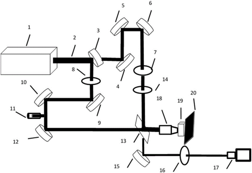
[0040] Such as figure 1 As shown, the femtosecond laser 2 with a center wavelength of 800 nanometers and a pulse width of 50 femtoseconds is output from the laser amplifier 1, and the vibration direction of the outgoing femtosecond laser is along the horizontal direction, which is a linearly polarized laser. Through the semi-transparent and semi-reflective lens 3, the single-beam femtosecond laser is converted into a double-beam femtosecond laser whose propagation directions are perpendicular to each other, and the double-beam femtosecond laser passes through the mirrors 4, 5, 6, 9, 10, 12 to change the propagation direction, The double beams of laser beams finally meet through the beam combining plate 13, and the reflector is adjusted so that the combined double beams propagate along a straight line in the same direction. Insert half-wave plate 7 in the optical path afterwards, make the polarization direction in this optical path change from horizontal polarization to vertica...

Embodiment 2

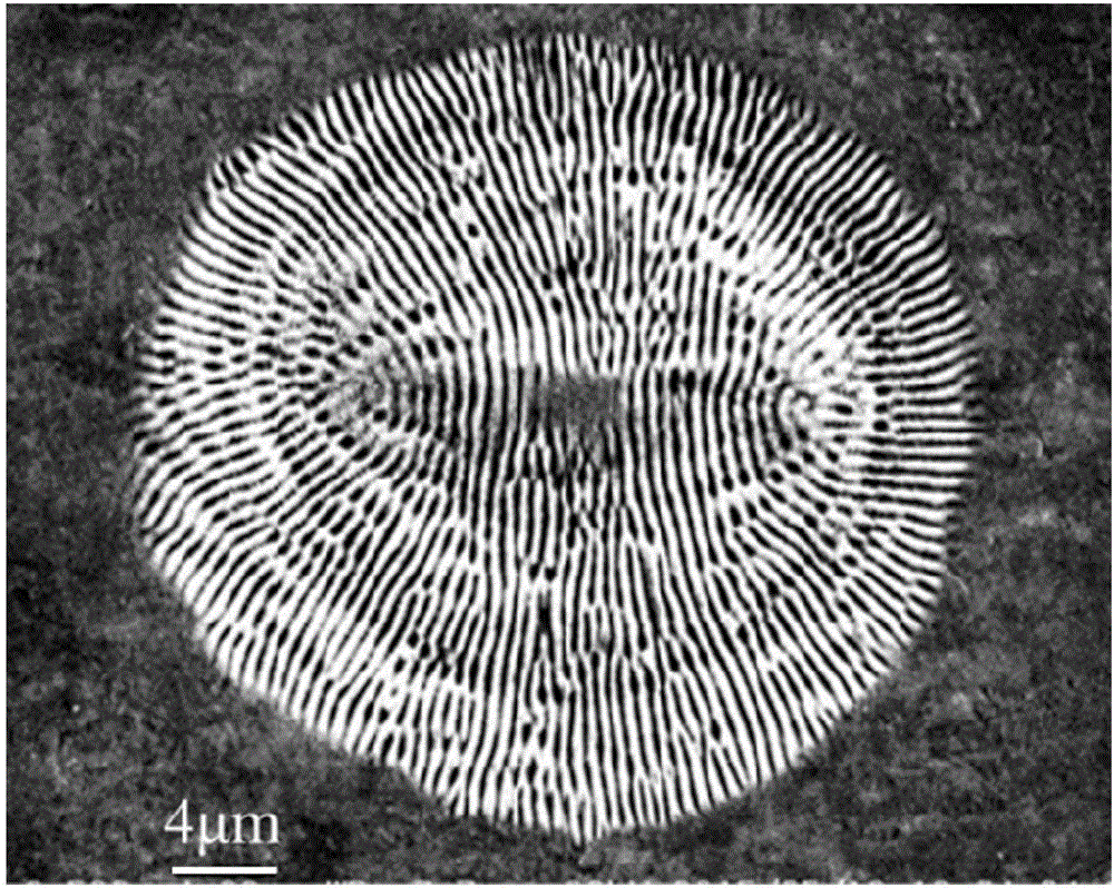
[0042] The metal target sample material is a metal tungsten sample material. On the basis of the optical path in Example 1, a neutral attenuation sheet 16 is used to adjust the laser power of the dual optical path so that the femtosecond laser of the dual optical path passes through the beam combining sheet. The power is equal, the total power of the measured laser is 2 microjoules, the metal tungsten sample target surface is 200 microns away from the focal point of the objective lens, when the delay time is 10 picoseconds, and the number of pulses N=100, the diameter obtained on the surface of the metal tungsten sample material is Scanning electron micrographs of 31 μm butterfly microstructures, as figure 2 Shown, where the magnification is 2500 times.

Embodiment 3

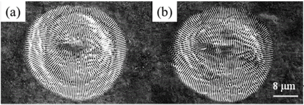
[0044] The metal target sample material is a metal tungsten sample material. On the basis of the optical path in Example 1, a neutral attenuation sheet is used to adjust the laser power of the dual optical path, so that the laser power of the femtosecond laser of the dual optical path exits through the beam combining sheet. Equal, at the position before they are incident on the focusing objective lens, the measured total laser power is 2 milliwatts micro-focus, the target surface of the metal tungsten sample is 200 microns away from the focal point of the objective lens, the number of pulses N=100, and the delay time is positive 5 pico The scanning electron micrographs of the butterfly microstructure were obtained on the surface of the metal tungsten sample material at minus 5 picoseconds, such as image 3 As shown in a and b, they are scanning electron micrographs of a butterfly microstructure with a diameter of 30 microns obtained on the surface of the sample material, and th...


PUM

PropertyMeasurementUnit
wavelengthaaaaaaaaaa
diameteraaaaaaaaaa

Abstract

The invention discloses a femtosecond laser direct writing preparation method of a two-dimensional submicron butterfly-shaped metal microstructure. The technical scheme comprises the following steps: (1) a metal target sample material is polished and mounted; (2) linear polarization and angular polarization double-pulse femtosecond laser capable of changing the delay time is obtained; (3) the point focusing of the double-pulse femtosecond laser is performed; (4) the position of the metal target sample material is adjusted; (5) the focal position of an objective lens is determined; (6) the surface of the metal target sample material is adjusted; and (7) the two-dimensional submicron butterfly-shaped metal microstructure is prepared. The method forms two linear polarization and angular polarization double-pulse femtosecond laser for homochromatic collinear transmission and capable of changing the delay time through skillfully using a light splitting method of a micronanometer machining platform, and adopts the objective lens point focusing mode to conveniently and quickly perform direct writing on the metal surface to prepare the two-dimensional submicron butterfly-shaped metal microstructure with bent stripe direction.

Description

technical field [0001] The invention relates to a method and a processing device for directly writing a two-dimensional submicron butterfly metal microstructure on the surface of a metal material with a femtosecond laser, wherein a micro-nano processing platform built by a Michelson interference system is used to form a collinear transmission in space and a delay in time Variable double-beam femtosecond laser, the double-beam femtosecond laser is focused through the objective lens, and then a new two-dimensional submicron butterfly metal microstructure is prepared on the surface of the material by dotting. This method and processing device belong to the field of ultrafast laser application and micro-nano processing, and have important potential applications in the design and preparation of new metal nanophotonic devices in the future. Background technique [0002] The preparation of micro-nano structures has shown important applications in industry and scientific research. D...

Claims


Application Information

Patent Timeline
Patent Type & Authority Applications(China)
IPC IPC(8): B23K26/362B23K26/067B23K26/064
CPCB23K26/0643B23K26/0648B23K26/0676B23K26/361
Inventor 乔红贞舒方杰杨涛李莉冀园园
Owner SHANGQIU NORMAL UNIVERSITY
Why Eureka
Try Eureka