Back-illuminated high-speed photodiode receiving chip and manufacturing method thereof

A photodiode and receiving chip technology, applied in circuits, electrical components, semiconductor devices, etc., can solve the problems of reduced chip photo-generated carrier quantum efficiency, low high-speed chip coupling efficiency, and low photo-generated quantum efficiency, and improved quantum efficiency. , The effect of reducing the transmission time and expanding the light absorption area

Active Publication Date: 2020-03-17
SHENZHEN PHOGRAIN INT TECH DEV
View PDF7 Cites 2 Cited by
  • Summary
  • Abstract
  • Description
  • Claims
  • Application Information

AI Technical Summary

Problems solved by technology

But this also leads to two defects at the same time: (1) too small area of ​​the chip diffusion source region will seriously affect the coupling efficiency of the chip and the input fiber during use. When the diameter of the chip source region is less than 20 μm, the chip will The coupling efficiency in the process will drop by about 50%; (2) the short chip InGaAs absorption layer length will cause the chip photogenerated carrier quantum efficiency η to decrease, according to the calculation formula η=1-exp(-αL) of the chip quantum efficiency, Among them, α is the absorption coefficient, which is determined by the material of the InGaAs absorbing layer of the chip and the receiving wavelength. It is basically a fixed value. Therefore, the smaller the length of the InGaAs absorbing layer, the lower the photogenerated quantum efficiency. At μm, the photogenerated carrier quantum efficiency of InGaAs material for 1310nm and 1550nm wavelength will be lower than 70%
[0005] In the prior art, the light receiving chip usually adopts such as figure 1 The chip structure shown in the normal incident mode, InP substrate 102', InP buffer layer 104', InGaAs absorbing layer 106', InP top layer 108', passivation film 110', anti-reflection film 112', diffusion source region 114 ', the chip positive electrode 116', the chip negative electrode 118', the incident light usually enters the chip from the upper surface of the chip diffusion source region 114', but in order to make the chip rate higher than 20GHz, the diameter D of the diffusion source region 114' is usually designed The length L of the InGaAs absorbing layer 106' of the chip is usually designed to be 1 μm to 1.5 μm. Therefore, high-speed chips with this structure generally have application defects such as low coupling efficiency and low quantum efficiency.

Method used


Image

  • Back-illuminated high-speed photodiode receiving chip and manufacturing method thereof
  • Back-illuminated high-speed photodiode receiving chip and manufacturing method thereof
  • Back-illuminated high-speed photodiode receiving chip and manufacturing method thereof

Examples


Embodiment Construction

[0047] In order to understand the above-mentioned purpose, features and advantages of the present invention more clearly, the present invention will be further described in detail below in conjunction with the accompanying drawings and specific embodiments. It should be noted that, in the case of no conflict, the embodiments of the present application and the features in the embodiments can be combined with each other.

[0048] In the following description, many specific details are set forth in order to fully understand the present invention, but the present invention can also be implemented in other ways different from those described here, therefore, the protection scope of the present invention is not limited to the specific details disclosed below. EXAMPLE LIMITATIONS.

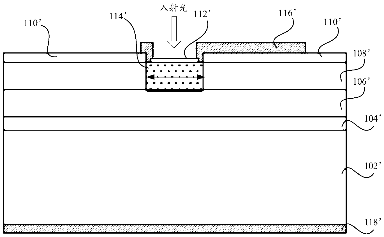
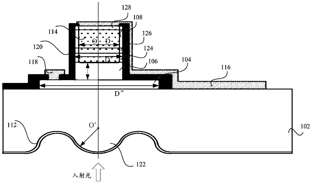
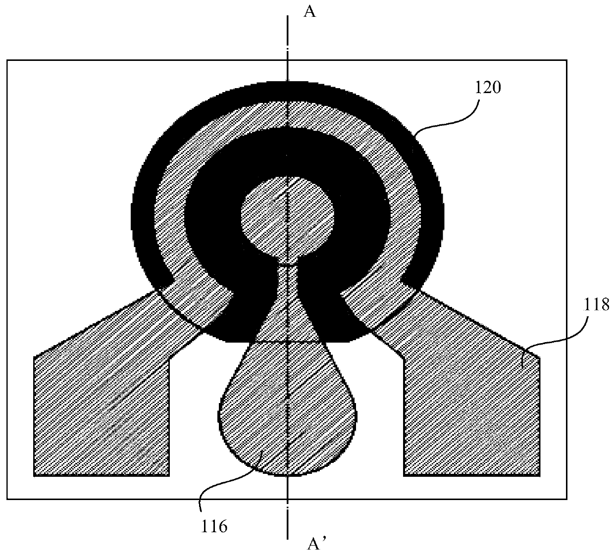
[0049] In the embodiment of the first aspect of the present invention, a back-illuminated high-speed photodiode receiving chip is proposed, figure 2 A schematic cross-sectional view showing the structur...


PUM

PropertyMeasurementUnit
thicknessaaaaaaaaaa
thicknessaaaaaaaaaa
diameteraaaaaaaaaa

Abstract

The invention provides a back lighting type photodiode receiving chip and a manufacturing method thereof. The chip comprises an epitaxial layer, the epitaxial layer comprises a P-shaped table face, an N-shaped table face and an indium phosphide substrate; the P-shaped table face comprises an InGaAs absorbing layer, an InGaAsP gradient layer, a reflective mirror layer, an indium phosphide top layer and an InGaAs contact layer; the N-shaped table face comprises an indium phosphide buffer layer; the indium phosphide buffer layer, the InGaAs absorbing layer, the InGaAsP gradient layer, the reflective mirror layer, the indium phosphide top layer and the InGaAs contact layer are grown on the indium phosphide substrate in sequence; an integrated micro lens is arranged at one side of the indium phosphide substrate, and the integrated micro lens and the indium phosphide buffer layer are at the different sides of the indium phosphide substrate. According to the back lighting type photodiode receiving chip and a manufacturing method, on the condition of guaranteeing that chip diffused source area keeps constant, the light absorption area of the chip is expanded, the problem of low coupling efficiency caused by small chip diffused source area is solved, and through the addition of the reflective mirror layer, the quantum efficiency of the chip can be improved.

Description

technical field [0001] The invention relates to the field of chip technology, in particular to a back-illuminated high-speed photodiode receiving chip and a manufacturing method thereof. Background technique [0002] With the promotion of fiber-to-the-home HTTP and the construction of 5G base stations, the demand for high-speed photodiode light-receiving chips is becoming increasingly urgent. At present, 10G high-speed photodiode receiving chips have become the mainstream products of current technology applications, and the demand for 25G, 100G, and 400G photodiode receiving chips is also in the rising stage of rapid development. [0003] The speed of the photodiode receiving chip mainly depends on two aspects: one is the transit time determined by the drift speed of the photo-generated carriers in the chip, such as the formula As shown, where υ is the drift velocity of photogenerated carriers, which is basically a fixed value of 6×106 cm / s, and L is the length of the InGa...

Claims


Application Information

Patent Timeline
Patent Type & Authority Patents(China)
IPC IPC(8): H01L31/102H01L31/0232H01L31/0352H01L31/0224H01L31/18
CPCH01L31/022408H01L31/02327H01L31/035236H01L31/102H01L31/1844
Inventor 杨彦伟陆一峰刘格刘胜宇刘宏亮
Owner SHENZHEN PHOGRAIN INT TECH DEV
Why Eureka
Try Eureka