

Preparation method of side incidence type SOI-based Si/SiGe HPT with photonic crystal structure
A photonic crystal, n-type technology, applied in semiconductor devices, final product manufacturing, sustainable manufacturing/processing, etc., can solve problems affecting performance and achieve low cost, easy implementation, and efficient absorption
- Summary
- Abstract
- Description
- Claims
- Application Information
AI Technical Summary
Problems solved by technology
Method used
Image

Examples
preparation example Construction
[0027] The invention provides a method for preparing a side-incidence SOI-based Si / SiGe HPT with a photonic crystal structure that takes into account both high-efficiency absorption and high-speed operation, comprising the following steps:
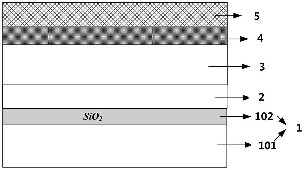
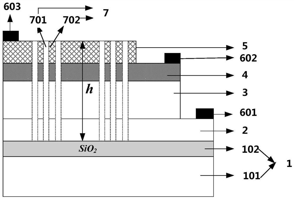
[0028] (1) On SOI substrate 1 (101-Si substrate; 102-SiO 2 Layer) on the epitaxial Si sub-collector region 2, Si collector region 3, Si x Ge 1-x Base region 4, polycrystalline Si emitter region 5.
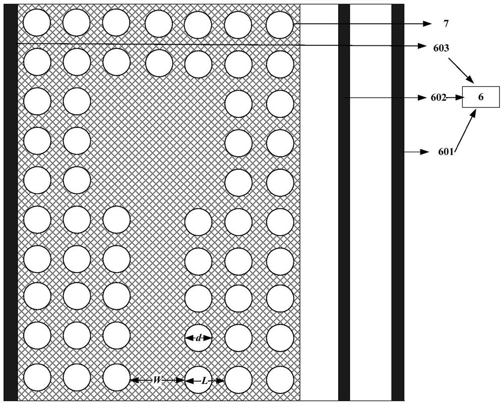
[0029] (2) Fabricate the photonic crystal structure 7 .
[0030] (3) Etching the base area and the mesa of the collector area.
[0031] (4) Deposit an insulating layer.
[0032] (5) Etching the contact hole.
[0033] (6) Metal electrodes 6 (601—collector electrode; 602—base electrode; 603—emitter electrode) are fabricated by photolithography to form ohmic contacts.
Embodiment 1
[0035] The invention provides a method for preparing a side-incidence SOI-based Si / SiGe HPT with a photonic crystal structure that takes into account both high-efficiency absorption and high-speed operation, comprising the following steps:
[0036] (1) Select a (100) Si wafer with a diameter of 4 inches, with a thickness of about 150um, perform oxygen ion implantation in the Si wafer to form a high-concentration oxygen implantation layer, and then perform high-temperature annealing to make the implanted oxygen and silicon Reaction to form SiO 2 Insulating layer, and finally get the SOI substrate through grinding and polishing. The n-type Si sub-collector region 2 and the n-type Si collector region 3 are successively grown on the SOI silicon wafer by low-pressure chemical vapor deposition (LPCVD), with thicknesses of 300nm and 600nm respectively, SiH 4 As Si source, the growth temperature is 700°C; As is used as n-type doping impurity source. Next, p-type Si is grown on the n...
Embodiment 2
[0043] The invention provides a method for preparing a side-incidence SOI-based Si / SiGe HPT with a photonic crystal structure that takes into account both high-efficiency absorption and high-speed operation, comprising the following steps:
[0044] (1) Select two Si wafers with a diameter of 4 inches (100) and a thickness of about 100um. Thermally oxidize, bond, and anneal the two wafers, and finally grind and polish them to about 15um to obtain an SOI substrate. The n-type Si sub-collector region 2 and the n-type Si collector region 3 were successively grown on the SOI silicon wafer by low-pressure chemical vapor deposition (LPCVD), with thicknesses of 300nm and 600nm respectively, SiH 4 As Si source, the growth temperature is 700°C; As is used as n-type doping impurity source. Then use reduced pressure chemical vapor deposition (RPCVD) to grow p-type Si on the n-type Si collector region 3 0.8 Ge 0.2 Base region 4, the thickness is 100nm, and the reaction source is SiH 4 a...
PUM
| Property | Measurement | Unit |
|---|---|---|
| Aperture | aaaaa | aaaaa |
| Thickness | aaaaa | aaaaa |
| Film thickness | aaaaa | aaaaa |
Abstract
Description
Claims
Application Information