Two-wire system built-in charge amplifying circuit based on field-effect tube
A charge amplifier circuit and field effect transistor technology, applied in charge amplifiers and other directions, can solve the problems of large volume, many signal noise sources, and reduce the signal-to-noise ratio of signal conversion, and achieve high load carrying capacity, wide application frequency response, and output. Low impedance effect
- Summary
- Abstract
- Description
- Claims
- Application Information
AI Technical Summary
Problems solved by technology
Method used
Image
Examples
Embodiment 1
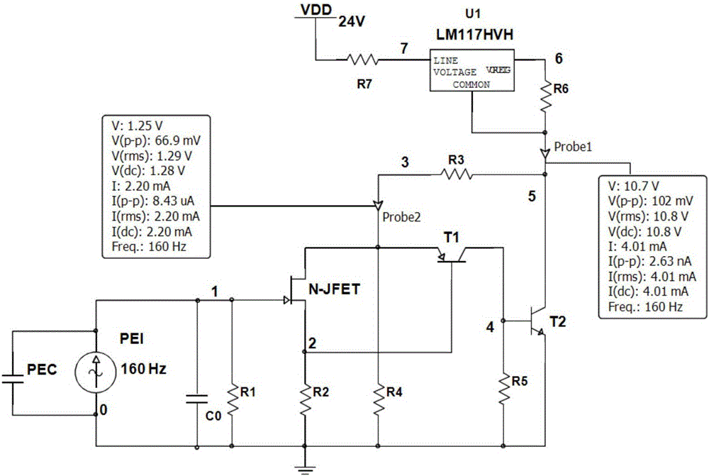
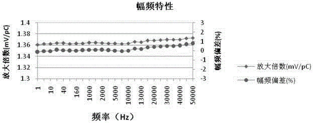
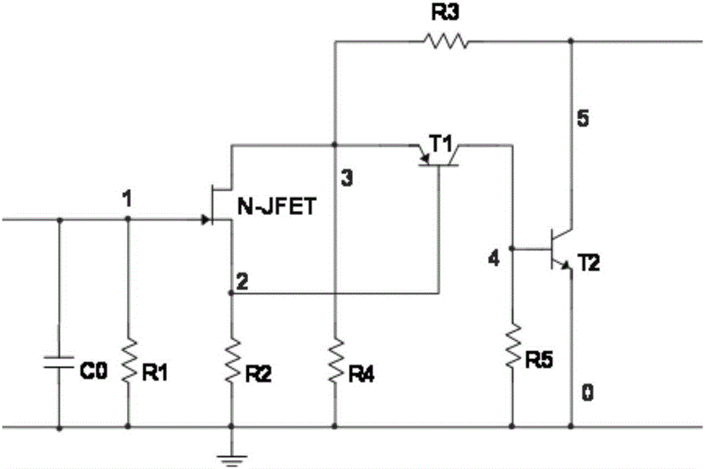
[0040] A certain type of charge output product of our company is jointly tested with a circuit adopting the structure and technology involved in the present invention, and the selection of triode components is J201, 9012 and 3904. The gain adjustment from 1mV / pC to 10mV / pC is realized, the circuit gain adjustment ability is not limited to this range, the gain frequency response deviation is less than 0.8% in the range of 50kHz, and the gain deviation in the 125°C range is less than 3%. The maximum shape of the circuit does not exceed Φ13.4mm×Φ6.1mm×2mm.
PUM
 Abstract
Description
Claims
Application Information
 - R&D
- Intellectual Property
- Life Sciences
- Materials
- Tech Scout
- Unparalleled Data Quality
- Higher Quality Content
- 60% Fewer Hallucinations
Browse by: Latest US Patents, China's latest patents, Technical Efficacy Thesaurus, Application Domain, Technology Topic, Popular Technical Reports.
© 2025 PatSnap. All rights reserved.Legal|Privacy policy|Modern Slavery Act Transparency Statement|Sitemap|About US| Contact US: help@patsnap.com


