Two-wire Built-in Charge Amplifying Circuit Based on Field Effect Transistor
A technology of charge amplification circuit and field effect tube, which is applied in the direction of charge amplifier, etc., can solve the problems of large volume, many signal noise sources, many stages of conversion amplification and adjustment, etc., and achieve small output impedance, high insulation resistance, and characteristic The effect of high frequency
- Summary
- Abstract
- Description
- Claims
- Application Information
AI Technical Summary
Problems solved by technology
Method used
Image
Examples
Embodiment 1
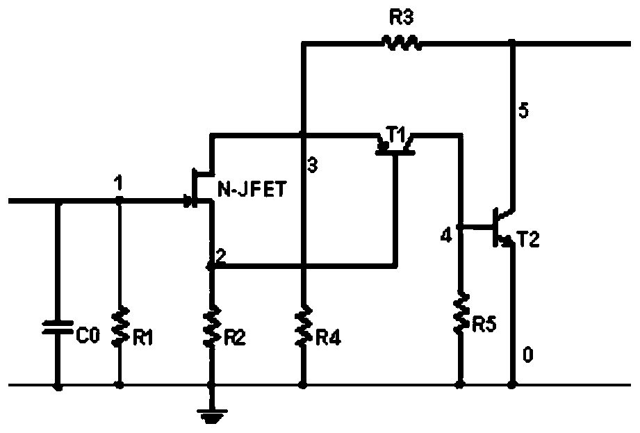
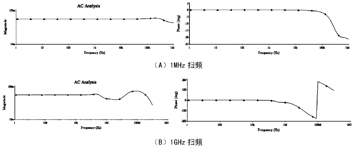
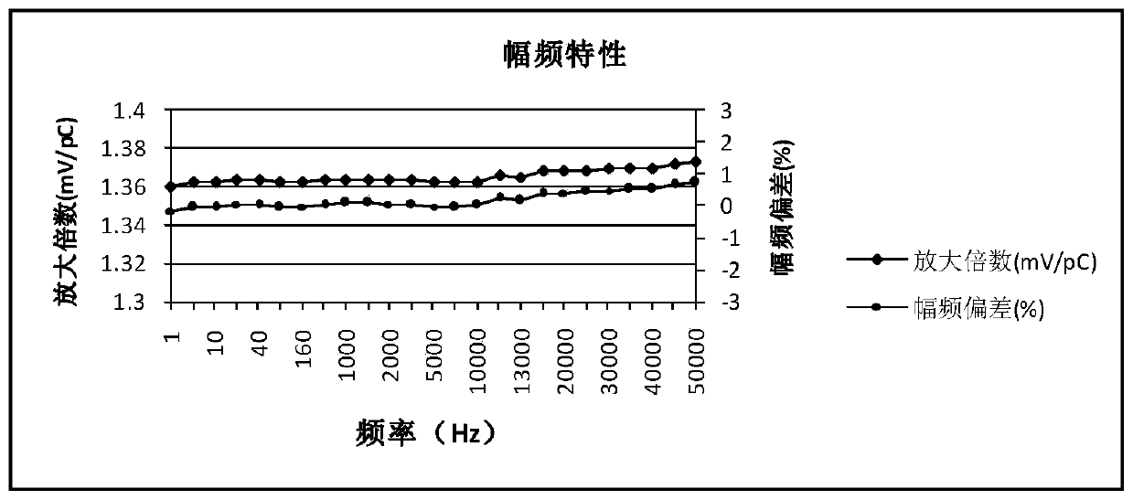
[0040] A certain type of charge output product of our company is jointly tested with a circuit adopting the structure and technology involved in the present invention, and the selection of triode components is J201, 9012 and 3904. The gain adjustment from 1mV / pC to 10mV / pC is realized, the gain adjustment capability of the circuit is not limited to this range, the gain frequency response deviation is less than 0.8% in the range of 50kHz, and the gain deviation in the 125°C range is less than 3%. The maximum shape of the circuit does not exceed Φ13.4mm×Φ6.1mm×2mm.
PUM
 Abstract
Description
Claims
Application Information
 - R&D
- Intellectual Property
- Life Sciences
- Materials
- Tech Scout
- Unparalleled Data Quality
- Higher Quality Content
- 60% Fewer Hallucinations
Browse by: Latest US Patents, China's latest patents, Technical Efficacy Thesaurus, Application Domain, Technology Topic, Popular Technical Reports.
© 2025 PatSnap. All rights reserved.Legal|Privacy policy|Modern Slavery Act Transparency Statement|Sitemap|About US| Contact US: help@patsnap.com


