Grooved PCB structure used for bare chip testing and manufacturing method thereof

A PCB board, bare chip technology, applied in the field of semiconductor integrated circuit testing, can solve the problems of metal PAD short circuit, conductive glue overflow, bare chip scrapping, etc., to avoid pollution, facilitate bonding, and avoid precision control problems.

Inactive Publication Date: 2017-05-31
NO 20 RES INST OF CHINA ELECTRONICS TECH GRP
View PDF5 Cites 9 Cited by
  • Summary
  • Abstract
  • Description
  • Claims
  • Application Information

AI Technical Summary

Problems solved by technology

The current PCB boards are mostly used to carry the packaged chips, and there is no PCB board design and processing specifically for carrying bare chip tests.
And the larger the area of ​​the bare chip, the more conductive glue is needed for direct bonding on the PCB. If too m

Method used


Image

  • Grooved PCB structure used for bare chip testing and manufacturing method thereof
  • Grooved PCB structure used for bare chip testing and manufacturing method thereof
  • Grooved PCB structure used for bare chip testing and manufacturing method thereof

Examples


Embodiment Construction

[0018] The present invention will be further described below in conjunction with the accompanying drawings and embodiments, and the present invention includes but not limited to the following embodiments.

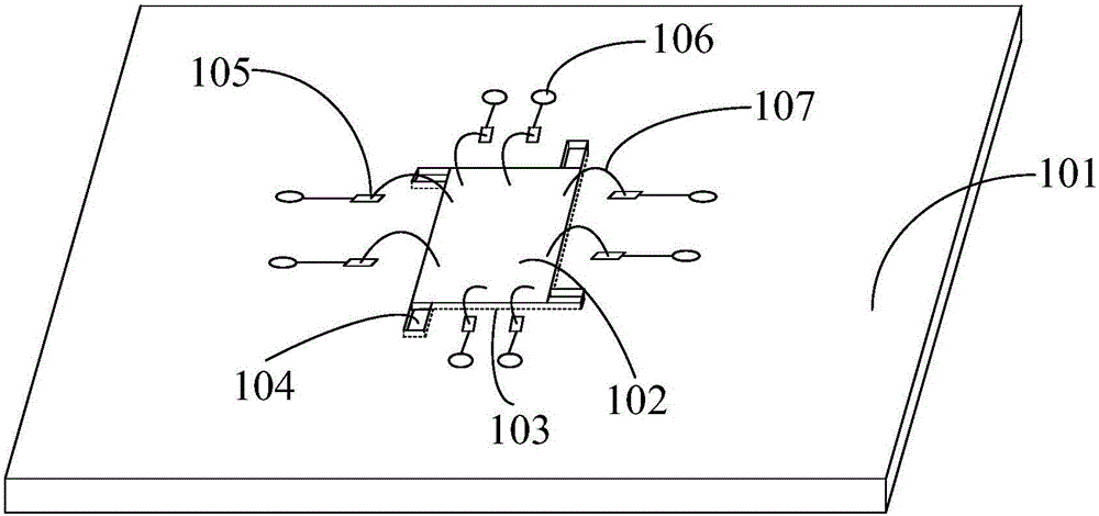
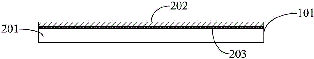
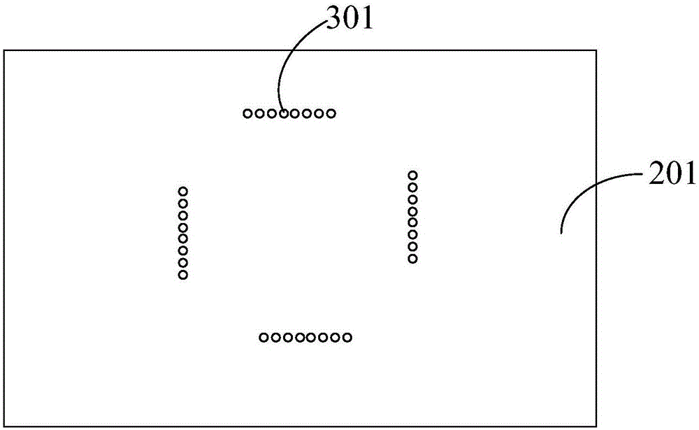
[0019] Such as figure 1 As shown, the present invention is composed of a PCB board 101 , a bare chip 102 , a groove 103 , an ear structure 104 , a metal pad 105 , a connection through hole 106 , and a bonding wire 107 . Such as figure 2 As shown, the PCB board 101 is composed of a first PCB board 201, a second PCB board 202, and an insulating medium layer 203. The insulating medium layer 203 is used for bonding between the first PCB board 201 and the second PCB board 202, while avoiding the first PCB board 201 and the second PCB board 202. The electrical short circuit between the first PCB board 201 and the second PCB board 202 . Such as image 3 As shown, the first PCB 201 is provided with a through-hole copper avoidance area 301, which is used to avoid the metal groun...


PUM


Abstract

The invention provides a grooved PCB structure used for bare chip testing and a manufacturing method thereof. The manufacturing method comprises the following steps: firstly machining a PCB, forming a groove of which the area and the shape are the same as those of a bare chip in the PCB, and machining a diversion trench and a bonding pad; then adding an insulating dielectric layer between two PCBs, and laminating the two PCBs, wherein no bonding pad is machined on the surface opposite to the two PCBs; using a drilling tool to form connecting through holes in the laminated PCBs; finally adhering a bare chip at the position of the groove, and adopting an ultrasonic-thermocompression welding bonding technology to complete golden wire bonding between metal PAD of the bare chip and the bonding pad on the PCBs. The structure is simple, low in cost and easy to machine, the design difficulty of the PCB is reduced, and the pollution for the metal PAD of the bare chip when a conducting resin overflows can be preferably avoided.

Description

technical field [0001] The invention relates to the field of semiconductor integrated circuit testing, in particular to a PCB board structure used for bare chip testing and a manufacturing method thereof. Background technique [0002] At present, after the chip tape-out is completed, the bare chip must be packaged in plastic material or ceramic material to provide environmental protection before it can be soldered on the PCB board for testing. As the competition in the electronic product market becomes more and more fierce, chip manufacturers need to launch chip products at a faster speed to occupy the early market and strive for more profits. However, the packaging cycle will take up valuable testing time and slow down the pace of product marketization. Wafer-level testing can test bare chips through wafer probes and special test benches, but only relatively simple testing tasks can be completed, and there are many limitations in testing the actual functions of chips. The...

Claims


Application Information

Patent Timeline
IPC IPC(8): H05K1/18H05K3/32H01L21/66
CPCH05K1/183H01L22/14H05K3/321H05K2203/06
Inventor 毕文婷舒钰
Owner NO 20 RES INST OF CHINA ELECTRONICS TECH GRP
Why Eureka
Try Eureka