

Ceramic package substrate manufacturing method and ceramic package substrate
A technology for ceramic substrates and ceramic packaging, applied in the field of ceramic packaging substrates and ceramic packaging substrates, can solve the problems of many equipment requirements, complex processes, expensive costs, etc., and achieve the effect of streamlining the process flow, reducing costs, and improving production efficiency.
- Summary
- Abstract
- Description
- Claims
- Application Information
AI Technical Summary
Problems solved by technology
Method used
Image

Examples
Embodiment 1
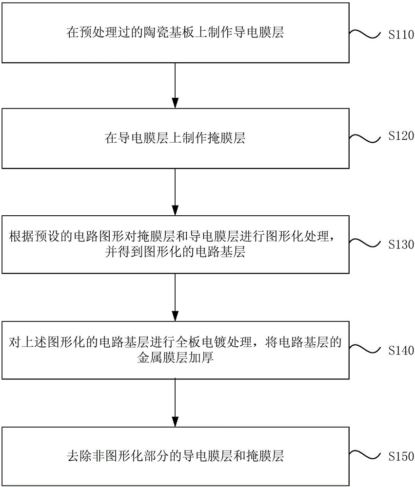
[0035] figure 1 It is a schematic flow chart of a manufacturing method of a ceramic package substrate provided in Embodiment 1 of the present invention. The manufacturing method of the ceramic packaging substrate in this embodiment can be used for the ceramic packaging substrate, meeting the increasingly stringent packaging requirements of the ceramic packaging substrate in the field of high-power, multi-chip device packaging.
[0036] The manufacturing method of the ceramic packaging substrate provided in this embodiment includes:
[0037] S110, fabricating a conductive film layer on the pretreated ceramic substrate.
[0038] Exemplarily, the pretreatment of the ceramic substrate includes at least one of surface microetching roughening, acid-base treatment, or ultrasonic cleaning. The ceramic substrate is pretreated by the above method, and then put into an oven for drying to remove the ceramic substrate. Impurities and dirt on the substrate surface. Nitrogen protection or...
Embodiment 2
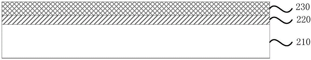
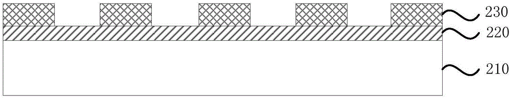
[0049] On the basis of the above embodiments, in the manufacturing method of the ceramic packaging substrate provided in this embodiment, the conductive film layer is a metal conductive film layer, and the mask layer is ink. The manufacturing method of the ceramic packaging substrate will be described below according to the steps of the process flow. figure 2 It is a side structural view of a ceramic substrate covered with a metal conductive film layer and a mask layer in sequence provided by Embodiment 2 of the present invention. Such as figure 2 As shown, the typical size of the ceramic substrate 210 is 114.3 mm in length, 114.3 mm in width, and 0.38 mm in thickness, and other sizes can also be selected.
[0050] The surface of the ceramic substrate 210 is treated, including micro-etching and roughening of the surface, acid-base treatment and ultrasonic cleaning, and then placed in an oven for drying. The oven is preferably nitrogen protection or a vacuum oven, and the dr...
Embodiment 3
[0059] On the basis of the above embodiments, in the manufacturing method of the ceramic packaging substrate provided in this embodiment, the conductive film layer is an organic conductive film layer, and the mask layer is ink. The manufacturing method of the ceramic packaging substrate will be described below according to the steps of the process flow. Figure 5 A side structure diagram of a ceramic substrate covered with an organic conductive film layer and a mask layer in sequence provided by Embodiment 3 of the present invention. Such as Figure 5 As shown, the typical size of the ceramic substrate 310 is 114.3 mm in length, 114.3 mm in width, and 0.38 mm in thickness, and other sizes can also be selected.
[0060] The surface of the ceramic substrate 310 is treated, including surface micro-etching roughening, acid-base treatment and ultrasonic cleaning, and then put into an oven for drying. The oven is preferably nitrogen protection or a vacuum oven, and the drying tempe...
PUM
| Property | Measurement | Unit |
|---|---|---|
| Thickness | aaaaa | aaaaa |
| Thickness | aaaaa | aaaaa |
| Thickness | aaaaa | aaaaa |
Abstract
Description
Claims
Application Information