Composite microwave dielectric material, printed circuit board base material made of composite microwave dielectric material and manufacturing method of composite microwave dielectric material
A technology of microwave dielectric materials and printed circuit boards, which is applied to printed circuits, dielectric materials, printed circuit dielectrics, etc., can solve the problems of poor mechanical properties, low bending strength, and large thermal expansion coefficient of polytetrafluoroethylene resin, etc., to achieve improved Effects of mechanical properties, reduction of thermal expansion coefficient, avoidance of circuit failure problems
- Summary
- Abstract
- Description
- Claims
- Application Information
AI Technical Summary
Problems solved by technology
Method used
Image

Examples
Embodiment 1
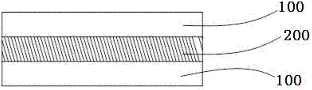
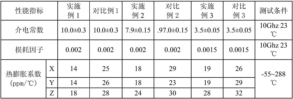
[0044] Such as figure 1 As shown, in this embodiment, the printed circuit board base material includes a composite microwave dielectric material plate 200 and metal foils 100 laminated on both sides thereof. In this application, the thickness of the metal foil and the thickness of the composite microwave dielectric material plate can be customized according to product requirements. In this embodiment of the present application, the metal foil layer 100 is a low-profile electrolytic copper foil, and the thickness of the metal foil layer 100 is 35 um. The thickness of the composite microwave dielectric material plate 200 is 0.25 mm. Its electrical performance parameters are shown in Table 1.
[0045] The manufacturing method of the printed circuit board base material of the present embodiment comprises the following steps:
[0046] Take by weighing 500 grams of PTFE emulsion (Daikin D210, PTFE solid content 60%), 700 grams of microwave dielectric ceramic powder filler (BaO-Sm...
Embodiment 2
[0054] Such as figure 1 As shown, in this embodiment, the printed circuit board base material includes a composite microwave dielectric material plate 200 and metal foils 100 laminated on both sides thereof. The metal foil layer 100 is a low-profile electrolytic copper foil, and the thickness of the metal foil layer 100 is 35um. The thickness of the composite microwave dielectric material plate 200 is 0.25 mm. Its electrical performance parameters are shown in Table 1.
[0055] The manufacturing method of the printed circuit board base material of the present embodiment comprises the following steps:
[0056] Take by weighing 100 grams of FEP emulsion (Daijin, FEP solid content 50%), 410 grams of PTFE emulsion (Daikin D210, PTFE solid content 60%) microwave dielectric ceramic powder filler 444 grams (BaO-ZnO-TiO 2 system, D50 particle size 5um, dielectric constant 36), use a mixer to mix for 1 hour, the speed is 1500 rpm, to obtain a uniformly mixed glue.
[0057] Add 200m...
Embodiment 3
[0064] Such as figure 1 As shown, in this embodiment, the printed circuit board base material includes a composite microwave dielectric material plate 200 and metal foils 100 laminated on both sides thereof. The metal foil layer 100 is a low-profile electrolytic copper foil, and the thickness of the metal foil layer 100 is 35um. The thickness of the composite microwave dielectric material plate 200 is 0.25mm. Its electrical performance parameters are shown in Table 1.
[0065] The manufacturing method of the printed circuit board base material of the present embodiment comprises the following steps:
[0066] Take by weighing 120 grams of PFA emulsion (Daikin, PFA solid content 50%), PTFE emulsion 400 grams (Daikin D210, PTFE solid content 60%) 200 grams of microwave dielectric ceramic powder filler (CaO-B 2 o 3 -SiO 2 system, D50 particle size 5um, dielectric constant 4.5), using a mixer to mix for 1 hour at a speed of 1500 rpm to obtain a uniformly mixed glue.
[0067] ...
PUM
| Property | Measurement | Unit |
|---|---|---|
| particle size | aaaaa | aaaaa |
| particle diameter | aaaaa | aaaaa |
| thickness | aaaaa | aaaaa |
Abstract
Description
Claims
Application Information
 - R&D
- Intellectual Property
- Life Sciences
- Materials
- Tech Scout
- Unparalleled Data Quality
- Higher Quality Content
- 60% Fewer Hallucinations
Browse by: Latest US Patents, China's latest patents, Technical Efficacy Thesaurus, Application Domain, Technology Topic, Popular Technical Reports.
© 2025 PatSnap. All rights reserved.Legal|Privacy policy|Modern Slavery Act Transparency Statement|Sitemap|About US| Contact US: help@patsnap.com