Wafer packaging structure for infrared focal plane array

A wafer-level packaging, infrared focal plane technology, applied in microstructure technology, microstructure devices, manufacturing microstructure devices, etc., can solve the problems of bulky structure, high cost, low assembly efficiency, etc., and achieve small size and cost. low effect

Inactive Publication Date: 2017-06-09
CHINA RESOURCES MICROELECTRONICS (CHONGQING) CO LTD
View PDF6 Cites 5 Cited by
  • Summary
  • Abstract
  • Description
  • Claims
  • Application Information

AI Technical Summary

Problems solved by technology

The structure of this package is bulky, the assembly efficiency is low, the difficulty is high, the cost is high, the mass production is difficult, and it is difficult to be used in the consumer electronics market

Method used


Image

  • Wafer packaging structure for infrared focal plane array
  • Wafer packaging structure for infrared focal plane array
  • Wafer packaging structure for infrared focal plane array

Examples


Embodiment 1

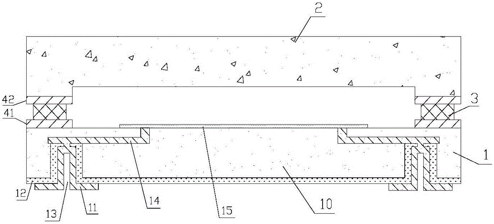
[0031] This embodiment proposes a wafer-level packaging structure of an infrared focal plane array, such as Figure 1 to Figure 4 As shown, it mainly includes:

[0032] An infrared detector chip 1, on which an infrared focal plane array 15 is arranged;

[0033] The infrared light window 2 is arranged on the infrared detector chip 1, and the edge of the infrared light window 2 is sealed and connected with the edge of the infrared detector chip 1, so as to form a vacuum chamber in which the vacuum air is sealed and connected to the infrared focal plane array 15;

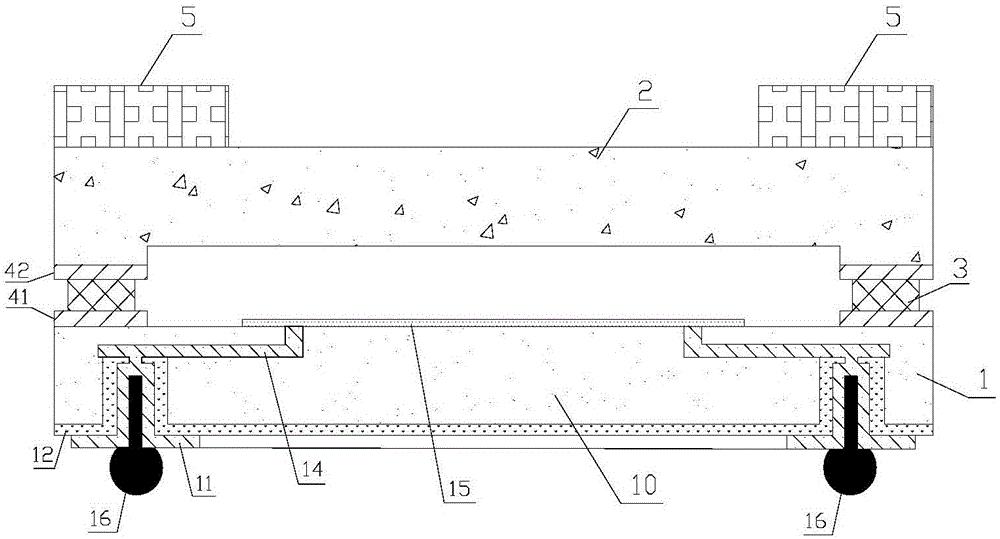
[0034] The lens 6 is arranged above the infrared light window 2 , and the edge of the lens 6 is sealed and connected with the edge of the infrared light window 2 .

[0035] On the basis of the above technical solution, as a preferred implementation mode, this embodiment uses an oxygen-free silicon wafer as the infrared window 2, and on both sides of the oxygen-free silicon wafer (ie, the infrared window 2), a An infr...

Embodiment 2

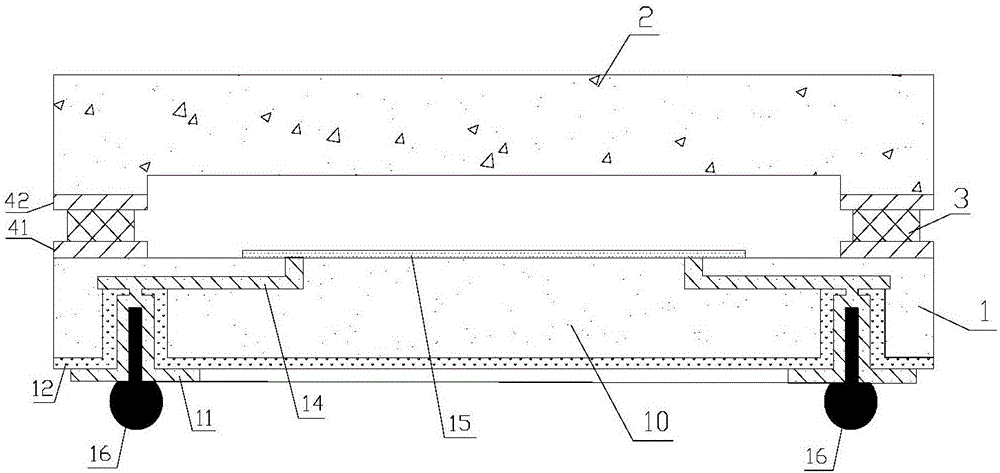
[0050] This embodiment proposes a packaging method for infrared focal plane arrays, based on the wafer-level packaging structure of Embodiment 1, such as Figure 1 to Figure 4 As shown, it mainly includes:

[0051] first step, such as figure 1 As shown, the edge of the silicon light window 2 and the edge of the infrared detector chip 1 are bonded by gold-tin eutectic solder 3 to form a vacuum cavity, and the conductive leads 14 of the infrared detector chip 1 are buried in the infrared detector chip 1. internal.

[0052] The second step, such as figure 2As shown, after thinning the second surface of the infrared detector chip 1 (that is, the lower surface in the figure), a deep hole 13 is opened on the second surface, and a passivation layer 12 and a metal layer are formed in the deep hole 13. The layer 11 and the passivation layer 12 serve as an insulating layer for electrical connection to insulate the metal layer 11 from the silicon substrate 10 , while the metal layer...


PUM


Abstract

The invention relates to the field of micro-electro mechanical system packaging and especially relates to a wafer packaging structure for an infrared focal plane array. The wafer packaging structure comprises an infrared detector chip, an infrared window and a lens, wherein the infrared focal plane array is arranged on the infrared detector chip; the infrared window is arranged on the infrared detector chip; an edge of the infrared window is in sealed connection with the edge of the infrared detector chip, so as to form a vacuum chamber for performing vacuum airtight sealing on the infrared focal plane array; the lens is arranged above the infrared window; the edge of the lens is in sealed connection with the edge of the infrared window. The wafer packaging structure for the infrared focal plane array, provided by the invention, has the advantages of small volume, low cost and large-scale production on the basis of a semiconductor technology; optical element integration is realized at wafer level; the requirements of commercial and consuming level applications for cost, volume and production scale can be met.

Description

technical field [0001] The invention relates to the field of micro-electromechanical system packaging, in particular to a wafer-level packaging structure of an infrared focal plane array. Background technique [0002] Infrared imaging technology is widely used in military, industrial, agricultural, medical, forest fire prevention, environmental protection and other fields, and its core component is the Infrared Focal Plane Array (IRFPA). [0003] The current packaging method of infrared focal plane array is mainly metal or ceramic vacuum packaging. The infrared optical window is used as a channel for infrared light to enter the focal plane array, and then the optical lens is assembled through external coupling to achieve the purpose of optical imaging. The structure of this package is bulky, the assembly efficiency is low, the difficulty is high, the cost is high, the mass production is difficult, and it is difficult to be used in the consumer electronics market. Contents ...

Claims


Application Information

Patent Timeline
Patent Type & Authority Applications(China)
IPC IPC(8): B81B7/02B81C1/00
CPCB81B7/02B81B2201/02B81C1/00261B81C1/00317
Inventor 吉涛
Owner CHINA RESOURCES MICROELECTRONICS (CHONGQING) CO LTD
Why Eureka
Try Eureka