Method for improving organic field effect transistor mobility through rapid annealing

A rapid annealing and mobility technology, which is used in the manufacture of electrical solid state devices, semiconductor devices, semiconductor/solid state devices, etc., to achieve the effect of easy preparation, optimization of mobility and surface energy

Inactive Publication Date: 2017-06-20
NANJING UNIV OF POSTS & TELECOMM
View PDF4 Cites 7 Cited by
  • Summary
  • Abstract
  • Description
  • Claims
  • Application Information

AI Technical Summary

Problems solved by technology

[0004] In order to solve the problem of regulating the interface properties and improving the mobility of organic field effect transistors by adjusting the molecular conformation of the polymer modification layer, the present invention proposes a method for performing rapid annealing on the polymer modification layer

Method used


Image

  • Method for improving organic field effect transistor mobility through rapid annealing
  • Method for improving organic field effect transistor mobility through rapid annealing
  • Method for improving organic field effect transistor mobility through rapid annealing

Examples


Embodiment 1

[0043] A method for rapid annealing to improve the mobility of an organic field effect transistor, comprising:

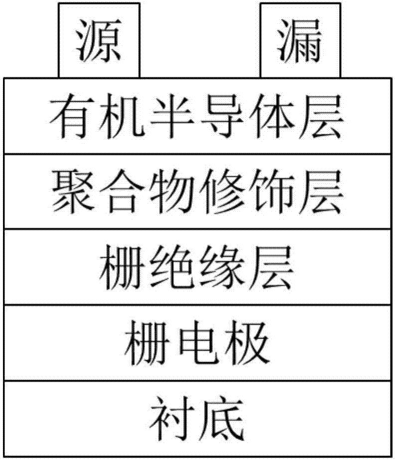
[0044] (1) Prepare an organic field-effect transistor with a polymer modification layer, the schematic diagram of which is shown in figure 1 shown;

[0045] It specifically includes the following steps: during actual preparation, the room temperature in the laboratory is kept at about 25° C., and the indoor humidity is kept below 30%.

[0046] (a) configuration polymer poly(4-vinylphenol) (PVP, molecular weight Mw=11kg / mol, T g =130°C) solution, PVP was formulated into a solution with ethyl acetate as a solvent, and the solubility was 3mg / ml;

[0047] (b) Select heavily doped silicon with 300nm silicon dioxide on the surface as the substrate and gate insulating layer, use acetone, ethanol, and deionized water to clean it with 100KHz ultrasonic waves for 10 minutes, and then dry it in a vacuum oven at 120°C ;

[0048] (c) putting the substrate dried in step (b) i...

Embodiment 2

[0054] A method for rapid annealing to improve the mobility of an organic field effect transistor, comprising:

[0055] (1) Prepare an organic field-effect transistor with a polymer modification layer, the schematic diagram of which is shown in figure 1 shown;

[0056] It specifically includes the following steps: during actual preparation, the room temperature in the laboratory is kept at about 25° C., and the indoor humidity is kept below 30%.

[0057] (a) configuration polymer polystyrene (PS, molecular weight Mw=250kg / mol, T g =100°C) solution, the PS is prepared into a solution with toluene as a solvent, and the solubility is 3mg / ml;

[0058] (b) Select heavily doped silicon with 300nm silicon dioxide on the surface as the substrate and gate insulating layer, use acetone, ethanol, and deionized water to clean it with 100KHz ultrasonic waves for 10 minutes, and then dry it in a vacuum oven at 120°C ;

[0059] (c) putting the substrate dried in step (b) into ultraviolet...


PUM


Abstract

The invention discloses a method for improving the organic field effect transistor mobility through rapid annealing. The method comprises the steps that a gate insulating substrate with a polymer modifying layer is prepared; rapid annealing is carried out on the gate insulating substrate; an organic semiconductor layer and source and drain electrodes are evaporated on the polymer modifying layer to prepare an organic field effect transistor; the transfer characteristic curve of the transistor is tested; the corresponding mobility is extracted; and the average mobility is calculated. The invention further provides the organic field effect transistor prepared by the method for improving the organic field effect transistor mobility through rapid annealing. The invention further provides the preparation method of the organic field effect transistor. According to the invention, the mobility of the organic field effect transistor is effectively improved through a simple solution processing technology, which is convenient for popularization and application.

Description

technical field [0001] The invention belongs to the technical field of organic field effect transistors in the semiconductor industry, and in particular relates to a method for improving the mobility of organic field effect transistors. Background technique [0002] As a basic component in electronic circuits, organic field-effect transistors are very suitable for the development of the next-generation flexible electronics industry because of their wide source of semiconductor layer materials, softness, and simple processing technology, and can be applied to large-area printing processes. In recent years, organic field-effect transistors have achieved rapid development, among which the mobility of single-crystal field-effect transistors based on rubrene has reached 15 cm 2 / Vs, has surpassed that of amorphous silicon. [0003] In organic field-effect transistors, the conductive channel is located in the sub-nanometer scale within the organic semiconductor layer close to the...

Claims


Application Information

Patent Timeline
Patent Type & Authority Applications(China)
IPC IPC(8): H01L51/40H01L51/05H01L51/00
CPCH10K71/00H10K71/40H10K10/00
Inventor 仪明东张晨曦陈艳李焕群凌海峰解令海黄维
Owner NANJING UNIV OF POSTS & TELECOMM
Why Eureka
Try Eureka