Small-signal model of super broadband gallium nitride device and parameter extraction method thereof

A small-signal model and parameter extraction technology, applied in the direction of instrumentation, electrical digital data processing, design optimization/simulation, etc., can solve problems such as poor accuracy, inapplicability, and large errors, and achieve the effect of easy operation and good stability

Inactive Publication Date: 2017-06-23
UNIV OF ELECTRONICS SCI & TECH OF CHINA
View PDF6 Cites 2 Cited by
  • Summary
  • Abstract
  • Description
  • Claims
  • Application Information

AI Technical Summary

Problems solved by technology

where C pga 、C pda 、C gda describes the parasitic capacitance caused by the metal pad, C pgi 、C pdi 、C gdi , L g , L d , L s Describes the parasitic capacitance and inductance caused by the gate, drain, and source metal electrodes, R d , R s describes the ohmic contact and channel resistance between a metal electrode and a semiconductor, R g The metal Schottky barrier resistance is described, and the designer of the equivalent circuit model applies it to the W band, and proposes a more reasonable parameter extraction method, that is, completely removes the influence of the excessively structured coplanar waveguide (CPW), only in The parasitic parameters are extracted in the case of HEMT zero bias and pinch-off, and all parasitic parameters can be obtained without any optimization algorithm, but the distribution effect of the device is not well resolved when describing the small signal characteristics, and then when describing the W-band HEMT small signal S The error obtained when the parameters are large
[0005] In summary, the small-signal equivalent circuit model proposed by Jarndal et al. is not suitable for the W frequency band because the parasitic parameter network is too simple. The equivalent circuit model proposed by Nguyen et al. is applied, focusing on the coplanar waveguide in the peel test The high-frequency effect on the device still uses a relatively simple parasitic parameter network, so the accuracy is poor, that is, the small-signal circuit model of the gallium nitride high electron mobility transistor in the prior art has a technical defect that is not suitable for the W-band

Method used


Image

  • Small-signal model of super broadband gallium nitride device and parameter extraction method thereof
  • Small-signal model of super broadband gallium nitride device and parameter extraction method thereof
  • Small-signal model of super broadband gallium nitride device and parameter extraction method thereof

Examples


Embodiment Construction

[0043] The following will clearly and completely describe the technical solutions in the embodiments of the present invention with reference to the accompanying drawings in the embodiments of the present invention. Obviously, the described embodiments are only some, not all, embodiments of the present invention. Based on the embodiments of the present invention, all other embodiments obtained by persons of ordinary skill in the art without making creative efforts belong to the protection scope of the present invention.

[0044] The purpose of the present invention is to provide a small signal model of an ultra-wideband gallium nitride device.

[0045] In order to make the above objects, features and advantages of the present invention more comprehensible, the present invention will be further described in detail below in conjunction with the accompanying drawings and specific embodiments.

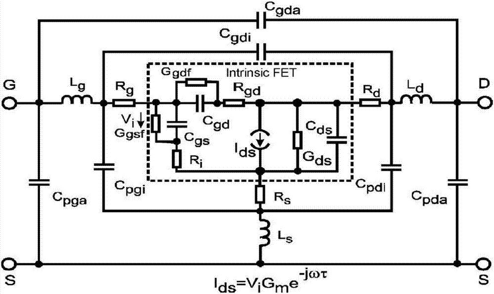
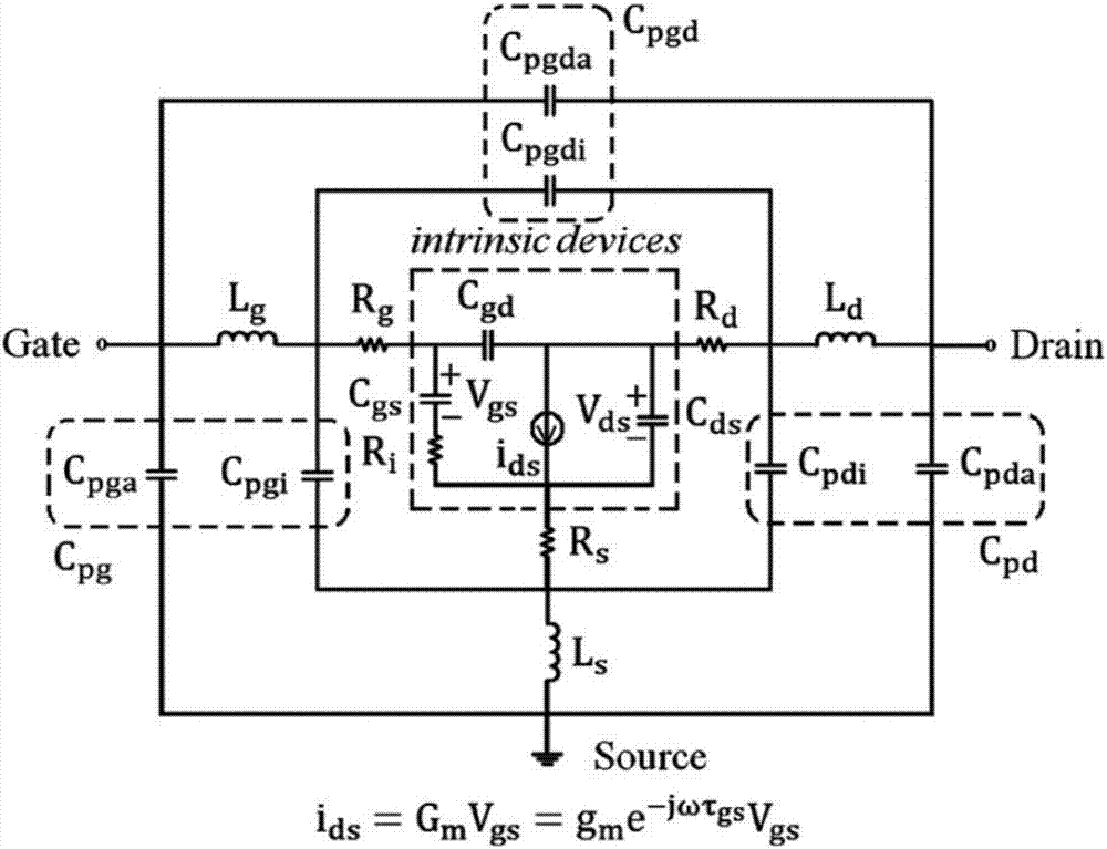
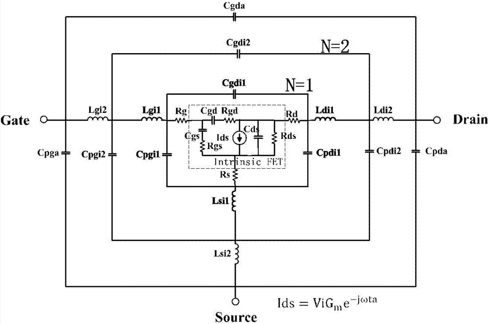
[0046] For the small-signal equivalent circuit model of an ultra-wideband (0.2GHz-110GH...


PUM


Abstract

The invention discloses a small signal model of the super broadband gallium nitride device and a parameter extraction method thereof. The small signal model in a bar, a source, and a leak end uses three interconnected capacitors and a cascadeinductance network structure formrespectively, and comprises 18 parasitic parameters and 10 intrinsic parameters; the parasitic parameterscomprise outer parasitic capacitors Cpgi1, Cpdi1, and Cgdi1 and the like, the parasitic inductancesLgi1, Ldi1, and Lsi1 and the like, andthe parasitic resistances Rg, Rd, and Rs; the intrinsic parameterscomprisethe intrinsic capacitors Cgd, Cgs and the Cds, the intrinsic resistances Rgs, Rgd, Rds, and the parameters Gm and ta in the intrinsic current source Ids=ViGme-jOmegata. The model can be used to accurately describe the characteristics of high-frequency devices, can makethe model to have a wider application band, the maximum can be applied to the w-frequency band; the parameter extraction method can achieve excellent stability in a 0.2-110GHz frequency range of the model parameters.

Description

technical field [0001] The invention relates to the technical field of microwave devices, in particular to a small-signal model of an ultra-wideband gallium nitride device and a parameter extraction method thereof. Background technique [0002] Gallium Nitride High Electron Mobility Transistor (GaN HEMT) is widely used in microwave circuits due to its high frequency and high power characteristics. Since GaN HEMTs need to work under high temperature and high power conditions, the large-signal equivalent circuit model is the basis for microwave circuit design using GaN HEMTs. In the bottom-up (bottomup) modeling method, an accurate small-signal model is the premise of establishing a large-signal model, so the small-signal model is an important link in the device modeling process. Due to the different working mechanisms of GaN HEMT devices, the small-signal models of first-generation semiconductor (silicon) and second-generation semiconductor (gallium arsenide, indium phosphid...

Claims


Application Information

Patent Timeline
Patent Type & Authority Applications(China)
IPC IPC(8): G06F17/50
CPCG06F30/20G06F30/367
Inventor 徐跃杭贾永昊毛书漫徐锐敏延波
Owner UNIV OF ELECTRONICS SCI & TECH OF CHINA
Why Eureka
Try Eureka