Two-dimensional conjugated polymer and preparation method and application thereof

A two-dimensional conjugated polymer technology, applied in the field of large-area ultra-thin two-dimensional conjugated polymer semiconductor materials and its preparation, can solve problems affecting film performance, polymer film wrinkles, limit application and development, etc., to achieve Ease of industrial application, mild reaction conditions, and simple operation

Active Publication Date: 2017-06-27
NANJING UNIV OF TECH
View PDF1 Cites 10 Cited by
  • Summary
  • Abstract
  • Description
  • Claims
  • Application Information

AI Technical Summary

Problems solved by technology

However, when the prepared large-area two-dimensional conjugated polymer is transferred to other insulating solid substrates for practical applications, wrinkles will also be introduced on the polymer film, which will affect the performance of the fil

Method used


Image

  • Two-dimensional conjugated polymer and preparation method and application thereof
  • Two-dimensional conjugated polymer and preparation method and application thereof
  • Two-dimensional conjugated polymer and preparation method and application thereof

Examples


Embodiment 1

[0047] Preparation of poly 9,9'-biscarbazole (Material I)

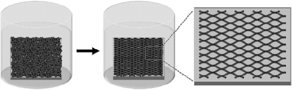
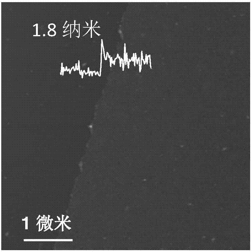
[0048] The schematic diagram of the polymerization reaction is as figure 1 As shown, the specific steps are as follows: 10 mg / mL of 9,9'-biscarbazole in chlorobenzene was spin-coated on a clean silica (300 nm) / silicon wafer (10 cm in diameter, measured by a plastic ruler ) substrate, spin-coating conditions are 500 rpm, 5 seconds and 2000 rpm, 30 seconds. The monomer-spin-coated substrate was then dried in an oven at 120° C. for 30 minutes. Then, at 25°C, soak the substrate in a dry dichloromethane solvent containing anhydrous ferric chloride, take it out after 24 hours of reaction, and wash the sample repeatedly with methanol, deionized water, concentrated hydrochloric acid, and dichloromethane in sequence . After drying in an oven at 50°C, a large-area ultrathin poly-9,9'-biscarbazole film grown on the substrate was obtained. The thickness of the obtained polymer film is about 1.8 nanometers ( figure 2 ).

Embodiment 2

[0050] Preparation of poly 4,4'-bis(N-carbazole)-1,1'-biphenyl (material Ⅲ)

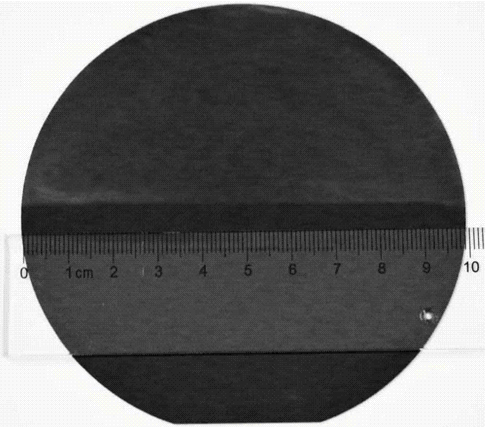
[0051] Spin-coat a 10 mg / mL solution of 4,4'-bis(N-carbazole)-1,1'-biphenyl in dichloromethane onto a clean silica (300 nm) / silicon wafer (10 cm in diameter) , measured by a plastic ruler) substrate, the spin coating conditions were 500 rpm for 5 seconds and 2000 rpm for 30 seconds. The monomer-spin-coated substrate was then dried in an oven at 120° C. for 30 minutes. Then, at 25°C, soak the substrate in a dry chloroform solvent containing anhydrous ferric chloride, take it out after 24 hours of reaction, and wash the sample repeatedly with methanol, deionized water, concentrated hydrochloric acid, and dichloromethane in sequence . After drying in an oven at 50°C, a large-area ultrathin poly 4,4'-bis(N-carbazole)-1,1'-biphenyl film grown on the substrate was obtained.

[0052] The prepared materials were photographed ( image 3 ), it can be seen from the figure that the upper half of the wafer is...

Embodiment 3

[0058] Preparation of poly 4,4'-bis(N-carbazole)thiophene (Material Ⅳ)

[0059] Spin-coat a 10 mg / mL solution of 4,4'-bis(N-carbazole)thiophene in dichloroethane onto a clean silica (300 nm) / silicon wafer (10 cm in diameter, measured by a plastic ruler ) substrate, spin-coating conditions are 500 rpm, 5 seconds and 2000 rpm, 30 seconds. The monomer-spin-coated substrate was then dried in an oven at 120° C. for 30 minutes. Then, at 25°C, soak the substrate in a dry toluene solvent containing anhydrous ferric chloride, take it out after 24 hours of reaction, and wash the sample repeatedly with methanol, deionized water, concentrated hydrochloric acid, and dichloromethane in sequence. After drying in an oven at 50°C, a large-area ultrathin poly 4,4'-bis(N-carbazole)thiophene film grown on the substrate was obtained. The obtained polymer film thickness is about 1.7 nanometers ( Figure 10 ).


PUM

PropertyMeasurementUnit
Thicknessaaaaaaaaaa
Thicknessaaaaaaaaaa
Diameteraaaaaaaaaa

Abstract

The invention discloses a two-dimensional conjugated polymer and a preparation method and application thereof and belongs to the field of polymer semiconductor materials. The two-dimensional conjugated polymer uses carbazole as a framework and has the structure (shown in the description) of a chemical formula selected from a general formula (I) or a general formula (II). The preparation method comprises the steps that a carbazole derivative is firstly spin-coated on a flat substrate, then the polymer spin-coated with a monomer is immersed in an organic solvent containing anhydrous ferric chloride, and large-scale ultra-thin conjugated polymer nanosheets are prepared through oxidative polymerization reaction assisted by the substrate. The size of the two-dimensional conjugated polymer reaches centimeter level, and the thickness of the polymer reaches several nanometers. The polymer can stably exist in acid, alkali and water, has absorption peaks in an ultraviolet region, has the advantages of blue light emission and the like and has the very good application prospect in the fields of organic photoelectric detection devices, organic luminescent devices, organic electrical storage, organic field effect transistors, organic sensors, organic nano devices and separating filter membranes and the like.

Description

technical field [0001] The invention belongs to the field of polymer semiconductor materials, and in particular relates to a large-area ultrathin two-dimensional conjugated polymer semiconductor material and its preparation method and application. Background technique [0002] Since the two-dimensional material graphene was separated out in 2004, its excellent performance and potential applications in electronic devices, energy, environment and other fields have aroused great research interest [Chem.Rev.2013,113,3766 -3798]. At the same time, many universities, research institutions and companies at home and abroad have also turned their research interests to the synthesis and application of other two-dimensional nanomaterials such as molybdenum disulfide, boron nitride and two-dimensional polymers [Nat.Nanotechnol.2014,9,768-779] . Graphene can be considered as a two-dimensional polymer, but its zero-bandgap characteristic limits its application in organic electronic devi...

Claims


Application Information

Patent Timeline
IPC IPC(8): C08G61/12C08J5/18C08L65/00
CPCC08G61/124C08G61/126C08G2261/11C08G2261/1422C08G2261/1424C08G2261/148C08G2261/18C08G2261/3241C08G2261/92C08G2261/94C08J5/18C08J2365/00
Inventor 刘举庆刘正东黄维宋梦亚居尚
Owner NANJING UNIV OF TECH
Why Eureka
Try Eureka