Method for preparing silver nanosheet-modified polyacrylonitrile nano-pillar array film SERS substrate

A nano-pillar array, polyacrylonitrile technology, applied in ion implantation plating, liquid chemical plating, coating and other directions, to achieve the effect of good SERS signal repeatability

Inactive Publication Date: 2017-07-07
ANHUI AGRICULTURAL UNIVERSITY
View PDF4 Cites 17 Cited by
  • Summary
  • Abstract
  • Description
  • Claims
  • Application Information

AI Technical Summary

Problems solved by technology

[0003] Chinese Patent Publication No. CN 104498881 A discloses a method for preparing a polyacrylonitrile nanostructure array flexible substrate modified by silver nanoparticles. Although it has achieved good detection sensitivity and signal uniformity, there is still room for improvement.

Method used


Image

  • Method for preparing silver nanosheet-modified polyacrylonitrile nano-pillar array film SERS substrate
  • Method for preparing silver nanosheet-modified polyacrylonitrile nano-pillar array film SERS substrate
  • Method for preparing silver nanosheet-modified polyacrylonitrile nano-pillar array film SERS substrate

Examples


preparation example Construction

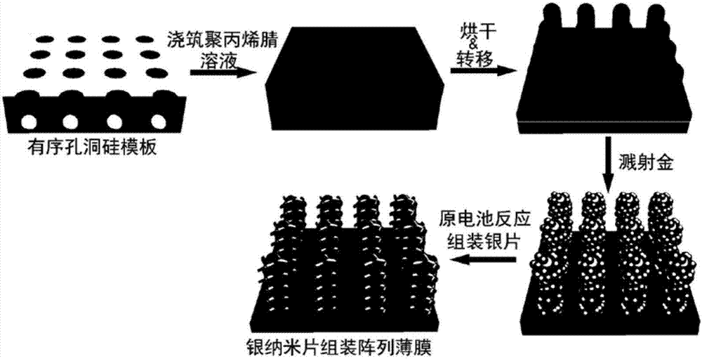
[0028] The preparation method of the polyacrylonitrile nanocolumn array film SERS substrate modified by silver nanosheets of the present invention comprises the following steps:

[0029] (1) First, pour a pre-configured amount (100-400 microliters) of a certain concentration of polyacrylonitrile solution (5%-10% mass fraction, the solvent is N,N'-dimethylformamide) On a silicon template with ordered nano-vertical holes (hexagonal or tetragonal arrangement of holes, period 100nm-1500nm, hole diameter 100nm-800nm, depth 100nm-600nm), and then heat it in an oven (60-80°C) Dry to remove the organic solvent, and after a certain period of time (20-30 minutes), peel off the upper layer of polyacrylonitrile film directly on the surface of the silicon template to obtain a PAN nanocolumn ordered array film;

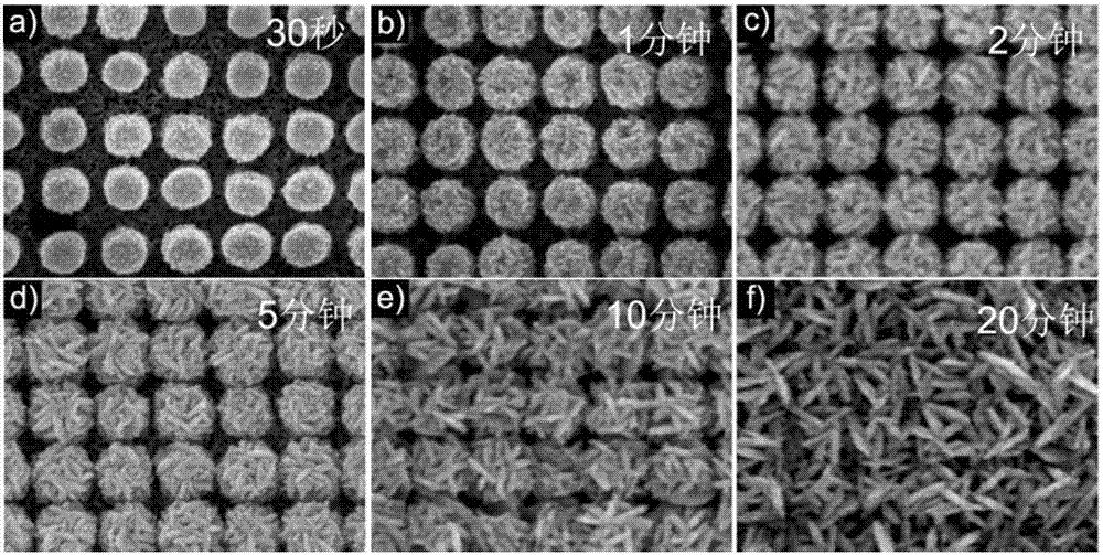
[0030](2) Using the ion sputtering method, sputtering gold nanoparticles on the surface of the PAN nanocolumn array film obtained in step (1) (2-5 minutes), to obtain the PAN nanoc...

Embodiment 1

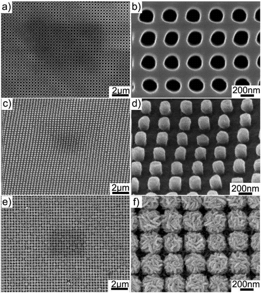
[0034] (1) Preparation of PAN nanopillar films: first, a silicon template with nanometer-sized vertical holes arranged in squares on the pre-prepared surface ( figure 2 a-b, period 350nm, diameter 225nm, depth 300nm; silicon template size 2cmx2cm) surface poured 300 microliters of polyacrylonitrile (mass fraction 8%, solvent is dimethylformamide (DMF) solution), and then coated with polyacrylonitrile The silicon template of the acrylonitrile solution was dried in an oven (70°C) to remove the DMF solution. After 25 minutes, a thin film was peeled off on the surface of the silicon template with tweezers to obtain a flexible film of polyacrylonitrile nanopillar arrays. Observation results from SEM ( figure 2 c-d) It can be seen that the surface of the polyacrylonitrile film has a large-area, regularly arranged array of nanocolumns. These nanocolumns are arranged in a uniform tetragonal array. The diameter of the nanocolumns is about 152 nm, and the distance between the centers ...

Embodiment 2

[0042] (1) Preparation of PAN nanopillar films: First, a silicon template with hexagonally arranged nano-vertical holes on the surface ( Figure 9 a-b, pore period 600nm, diameter 400nm, depth 680nm; silicon template size 2cmx2cm) pour 300 microliters of polyacrylonitrile (mass fraction 8%, solvent is dimethylformamide (DMF) solution) on the surface, and then coat the surface with The silicon template of the polyacrylonitrile solution was dried in an oven (70°C) to remove the DMF solution. After 25 minutes, a layer of film was peeled off on the surface of the silicon template with tweezers to obtain a flexible film of polyacrylonitrile nanopillar arrays. Observation results from SEM ( Figure 9 c-d) It can be seen that the surface of the polyacrylonitrile film has a large-area, regularly arranged array of nanopillars. These nanopillars are arranged in a uniform hexagonal array. The diameter of the nanopillars is about 270 nm, and the distance between the centers is about 600 n...


PUM

PropertyMeasurementUnit
diameteraaaaaaaaaa
depthaaaaaaaaaa
diameteraaaaaaaaaa

Abstract

The invention relates to a method for preparing a silver nanosheet-modified polyacrylonitrile nano-pillar array film SERS substrate. The method comprises the following steps that polyacrylonitrile solution is poured on a silicon template with ordered nanoporous vertical holes and is dried, after cooling, a polyacrylonitrile film of the upper layer is obtained, and namely a PAN nano-pillar ordered array film can be obtained; an ion sputter method is adopted, gold nanoparticles are spurted on the surface of the obtained PAN nano-pillar ordered array film, and namely the PAN nano-pillar ordered array film spurted by the gold nanoparticles is obtained; and the film modified by the gold nanoparticles is connected with a cooper sheet to be placed in mixed deposition fluid of silver nitrate and citric acid, and a silver nanosheet is deposited on the surface of the PAN nano-pillar by in situ pool reaction, so that the silver nanosheet-modified polyacrylonitrile nano-pillar array film SERS substrate is constructed. The substrate obtained by the method has good SERS signal repeatability, detection sensitivity and signal uniformity.

Description

technical field [0001] The invention relates to a preparation method of a SERS substrate. Background technique [0002] Raman (Raman) scattering spectrum can provide molecular vibration information, so it has the effect of fingerprint identification, and has very great application prospects in the fields of chemistry, biology, and environment. However, the ordinary Raman scattering effect is very weak, and the Raman scattered light intensity is about 10 of the incident light intensity. -6 -10 -9 ; In addition, during the Raman detection process, the Raman signal is easily interfered by the fluorescence signal, thus limiting the application of the Raman scattering detection technology in the above-mentioned fields. The surface-enhanced Raman scattering (SERS) effect based on gold, silver and other noble metal nanostructures can amplify the ordinary Raman detection signal by 1 million times. extensive attention. Among them, the SERS substrate based on noble metal nanostruc...

Claims


Application Information

Patent Timeline
Patent Type & Authority Applications(China)
IPC IPC(8): C23C14/34C23C14/20C23C18/42G01N21/65C08J7/06C08L33/20
CPCC08J7/06C08J2333/20C23C14/205C23C14/34C23C18/42G01N21/658
Inventor 李中波杜兆芳
Owner ANHUI AGRICULTURAL UNIVERSITY
Why Eureka
Try Eureka