High-electron-mobility transistor and memory chip

A high electron mobility, transistor technology, applied in semiconductor devices, circuits, electrical components, etc., can solve the problem of reverse leakage of devices, affecting the reliability of high electron mobility transistors, etc.

Inactive Publication Date: 2017-07-07
PEKING UNIV +2
View PDF4 Cites 0 Cited by
  • Summary
  • Abstract
  • Description
  • Claims
  • Application Information

AI Technical Summary

Problems solved by technology

[0005] However, the use of GaN materials and non-doped intrinsic materials causes serious reverse leakage in the device due to its interface state, which seriously affects the reliability of high electron mobility transistors

Method used


Image

  • High-electron-mobility transistor and memory chip
  • High-electron-mobility transistor and memory chip
  • High-electron-mobility transistor and memory chip

Examples


Embodiment 1

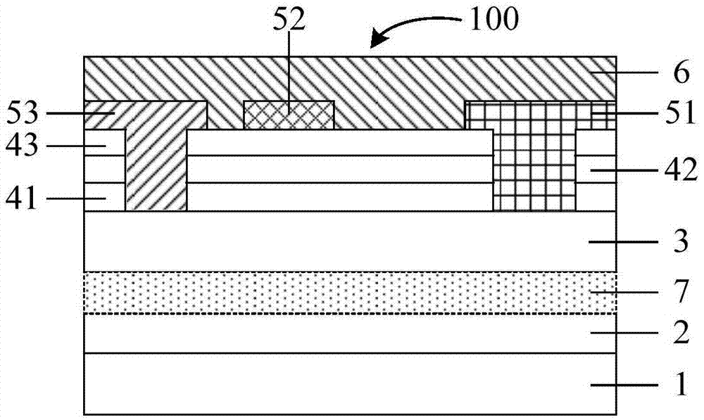
[0034] Such as figure 1 As shown, the dielectric layer includes a first silicon nitride layer 41 and a high-K metal oxide layer 43 sequentially from bottom to top.

Embodiment 2

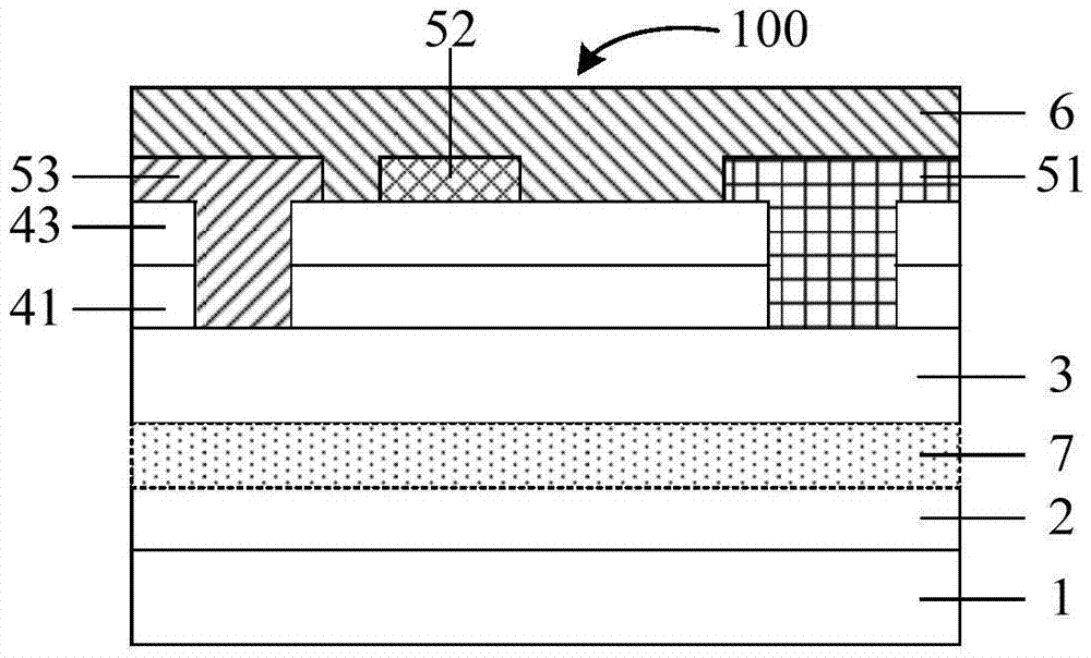
[0036] Such as figure 2 As shown, the dielectric layer sequentially includes a first silicon nitride layer 41 , a first silicon oxide layer 42 and a high-K metal oxide layer 43 from bottom to top.

Embodiment 3

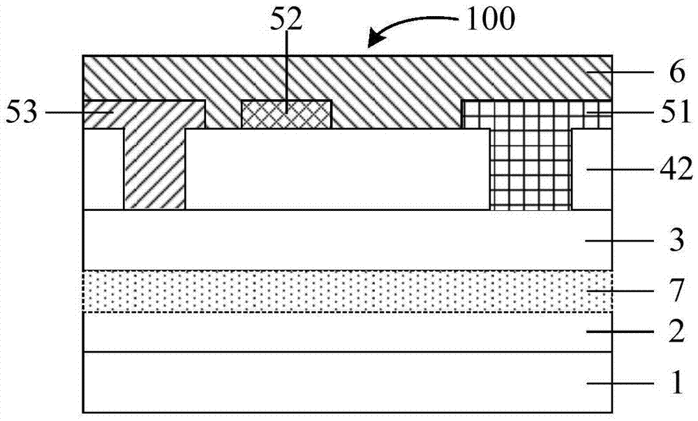
[0038] Such as image 3 As shown, the dielectric layer only includes the first silicon oxide layer 42, wherein the first silicon oxide layer 42 is also a high-K compound, which can also ensure the withstand voltage characteristics of the high electron mobility transistor 100, and at the same time, reduce the manufacturing difficulty and thin film stress.

[0039] In the above technical solution, preferably, the metal oxide layer 43 includes at least one of a hafnium oxide layer, a zirconium oxide layer, a titanium oxide layer, an aluminum oxide layer and a thallium oxide layer.

[0040] In this technical solution, by setting the metal oxide layer 43 to include at least one of a hafnium oxide layer, a zirconium oxide layer, a titanium oxide layer, an aluminum oxide layer and a thallium oxide layer, various implementations for improving the interface state are provided. Metal oxides have high capacitive properties and insulating properties.

[0041] In the above technical solu...


PUM


Abstract

The invention provides a high-electron-mobility transistor and a memory chip. The high-electron-mobility transistor comprises a substrate, a gallium nitride layer, a gallium nitride aluminum layer, a dielectric layer and an electrode, wherein one side of the gallium nitride layer is compounded on a surface layer of the substrate and the other side of the gallium nitride layer is compounded on a bottom portion of the gallium nitride aluminum layer; the dielectric layer is compounded on a top layer of the gallium nitride aluminum layer, and the dielectric layer is provided with at least two cut-through contact holes; the electrode includes a drain electrode, a gate electrode and a source electrode, and the drain electrode and the source electrode are arranged in the corresponding contact holes of the at least two corresponding cut-through contact holes; and the dielectric layer includes a metal oxide layer and/or an inorganic oxide layer, and the inorganic oxide layer includes a first silicon oxide layer. In the technical scheme, an interface state of the high-electron-mobility transistor is improved, a reverse direction leakage current of the transistor is effectively reduced and simultaneously reliability of the transistor is increased.

Description

technical field [0001] The invention relates to the technical field of semiconductors, in particular to a high electron mobility transistor and a memory chip. Background technique [0002] In related technologies, with the development of semiconductor manufacturing technology, power devices with low power consumption and high-speed high-pass characteristics have become the mainstream research direction. [0003] GaN (Gallium Nitride) is the third generation wide bandgap semiconductor material with large bandgap (3.4eV), high electron saturation rate (2e7cm / s), high breakdown electric field (1e10--3e10V / cm), relatively It has high thermal conductivity, corrosion resistance and radiation resistance, and has strong advantages in high pressure, high frequency, high temperature, high power and radiation resistance environmental conditions, so it is considered to be a research tool for short-wave optoelectronic devices and high-voltage, high-frequency and large Optimal material f...

Claims


Application Information

Patent Timeline
Patent Type & Authority Applications(China)
IPC IPC(8): H01L29/778H01L29/06
CPCH01L29/778H01L29/0657H01L2229/00
Inventor 刘美华陈建国林信南
Owner PEKING UNIV
Why Eureka
Try Eureka