Semiconductor structure and formation method therefor

A semiconductor, multi-layer structure technology, applied in the direction of semiconductor devices, semiconductor/solid-state device manufacturing, semiconductor/solid-state device components, etc., can solve the problem of easy cracking of the dielectric layer, achieve easy cracking, reduce the probability of cracking, low stress effect

Active Publication Date: 2017-07-14
SEMICON MFG INT (SHANGHAI) CORP +1
View PDF3 Cites 0 Cited by
  • Summary
  • Abstract
  • Description
  • Claims
  • Application Information

AI Technical Summary

Problems solved by technology

[0005] The problem solved by the present invention is to provide a semiconductor structure and its formation method, which can solve the problem that the dielectric layer is easy to crack

Method used


Image

  • Semiconductor structure and formation method therefor
  • Semiconductor structure and formation method therefor
  • Semiconductor structure and formation method therefor

Examples


Embodiment Construction

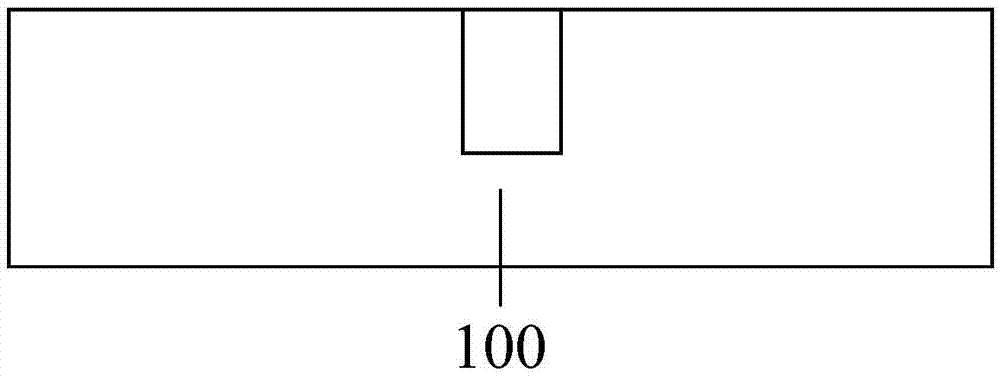
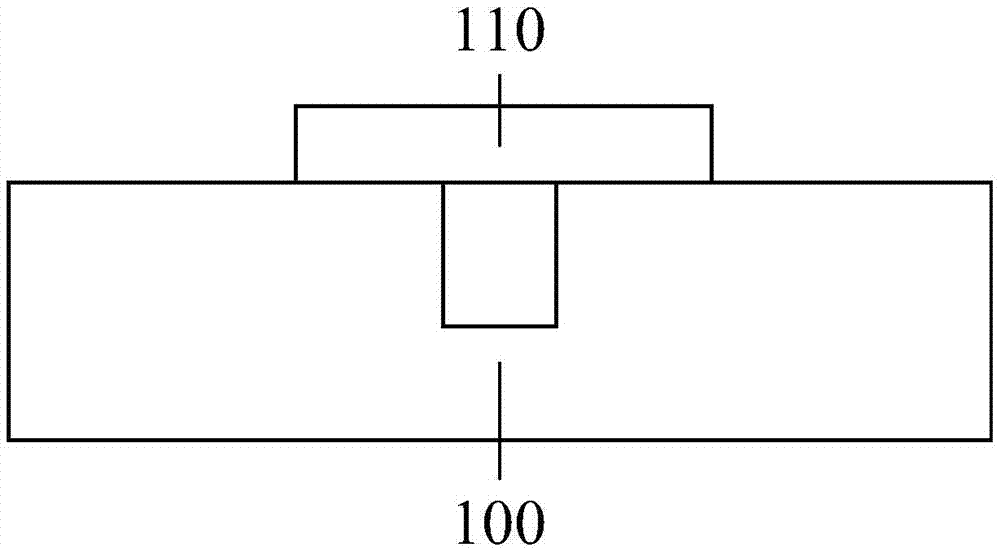
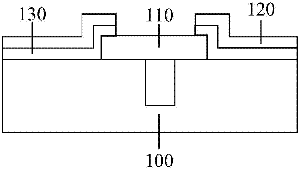
[0036] There are many problems in the semiconductor structure in the packaging process of the prior art, for example, the dielectric layer in the semiconductor structure is easy to crack.

[0037] In the prior art packaging process, the dielectric layer is usually a silicon nitride layer. In the process of forming the silicon nitride layer, the reactants include gas containing hydrogen atoms, which easily makes the silicon-hydrogen bond in the formed silicon nitride layer The content is higher. However, the silicon-hydrogen bond is unstable, and it is easy to break during the high-temperature process during the formation of the semiconductor structure. As a result, more dangling bonds are formed in the silicon nitride layer, resulting in poor stability of the silicon nitride layer and easy occurrence of cracks. In addition, the silicon nitride layer with high silicon-hydrogen bond content is prone to warping and deformation, resulting in cracking of the silicon nitride layer ...


PUM


Abstract

The present invention provides a semiconductor structure and a method for forming the same. The method for forming the semiconductor structure includes: providing a substrate; forming a spacer on the substrate, and the spacer includes a first surface opposite to the substrate , a second face opposite to the first face, and a side face between the first face and the second face, where the second face meets the side face as an edge; a hydrogen-containing reactant is used to form a cover covering the substrate and the second face The dielectric layer of the edge, the dielectric layer contains silicon-hydrogen bonds, and the dielectric layer includes: a first dielectric layer covering the substrate and the edge, and the silicon-hydrogen bonds in the first dielectric layer occupy The mole percentage is less than 2.8%. Wherein, by reducing the content of silicon-hydrogen bonds in the first silicon nitride layer, the first silicon nitride layer is not easy to generate dangling bonds, thereby increasing the stability of the silicon nitride layer; in addition, the low silicon-hydrogen bond content The warpage and deformation of the silicon nitride film is small under external influence, so the silicon nitride layer is not easy to produce cracks.

Description

technical field [0001] The invention relates to the technical field of semiconductor manufacturing, in particular to a semiconductor structure and a forming method thereof. Background technique [0002] With the continuous development of semiconductor technology, the size of integrated circuits is gradually reduced. The continuous shrinking of semiconductor geometry has also brought challenges to the semiconductor packaging process. [0003] Packaging (Package) is the process of assembling integrated circuits into chip final products. Specifically, the steps of packaging include: first forming an integrated circuit device, such as a transistor, etc. on a semiconductor substrate; then forming a metal interconnection structure connecting the above-mentioned integrated circuit device on the integrated circuit device; solder pads, and form solder balls on the solder pads, so as to electrically connect the chip structure to the printed circuit board or electrically connect two ...

Claims


Application Information

Patent Timeline
Patent Type & Authority Applications(China)
IPC IPC(8): H01L21/56H01L23/29H01L23/31
CPCH01L21/56H01L23/291H01L23/31
Inventor 高长城陈其道张京晶
Owner SEMICON MFG INT (SHANGHAI) CORP
Why Eureka
Try Eureka