
Method for preparing silicon carbide ohmic contact by adopting ion implantation enhanced laser annealing

A technology of ohmic contact and ion implantation, which is applied in the manufacture of semiconductor/solid-state devices, electrical components, circuits, etc., can solve the problems of poor process control, uneven ohmic contact resistivity, high ohmic contact resistivity, etc., to reduce resistivity, Reduce process control issues and improve performance results

Pending Publication Date: 2017-08-08
FOSHAN XINGUANG SEMICON
View PDF3 Cites 2 Cited by
  • Summary
  • Abstract
  • Description
  • Claims
  • Application Information

AI Technical Summary

Problems solved by technology

[0006] However, due to the uniformity of the laser spot, the formation of ohmic contacts on SiC by laser annealing faces the problems of poor process control, high ohmic contact resistivity, and uneven ohmic contact resistivity.

Method used


Image

  • Method for preparing silicon carbide ohmic contact by adopting ion implantation enhanced laser annealing
  • Method for preparing silicon carbide ohmic contact by adopting ion implantation enhanced laser annealing

Examples


Embodiment

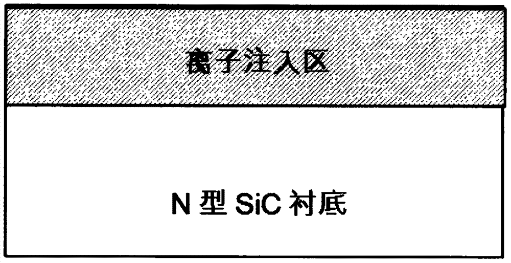
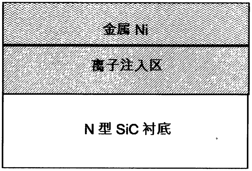
[0025] First, at the bottom of the N-type SiC substrate, a heavily doped region with a depth of 0.2 μm and a doping concentration of 1E20cm-3 is formed by ion implantation of N. The doping type of the part required to form an ohmic contact can be n-type doping , can also be P-type doping, and the doping type formed by the implanted ions is the same as the original doping type. For example: if the ohmic contact part is originally N-type doped, the implanted ions are one or more of N, P, As, etc. implanted together; if the ohmic contact part is originally P-type doped, the implanted ions are B, P, As, etc. One or more co-implantation of Al, etc.; ion implantation can be single-energy ion implantation or multiple-energy ion implantation, the depth of the heavily doped region formed after the ion implantation ranges from 0.01-1 μm, and the heavily doped Zone concentration range is 1E17cm -3 -5E21cm -3 , as attached figure 1 shown.

[0026] Then, a layer of Ni with a thickness ...


PUM

PropertyMeasurementUnit
Wavelengthaaaaaaaaaa

Abstract

The invention discloses a method for preparing silicon carbide ohmic contact by adopting ion implantation enhanced laser annealing. The method comprises the following steps of 1, performing ion implantation on a part, which needs to form ohmic contact, of SiC; 2, depositing ohmic contact metal on the surface of a SiC wafer; and 3, performing laser irradiation on the ohmic contact metal to form ohmic contact. By virtue of ion implantation, the doping concentration of the SiC ohmic contact region can be improved; by virtue of laser annealing, ohmic contact is formed on the SiC during activating the injected ions; and by adoption of the method, the process control problem in forming ohmic contact through the laser annealing process can be reduced and ohmic contact electrical resistivity is lowered, thereby improving the performance of the SiC device.

Description

technical field [0001] The invention relates to the field of silicon carbide device manufacturing, in particular to a method for preparing silicon carbide ohmic contacts by using ion implantation enhanced laser annealing. Background technique [0002] As a third-generation semiconductor material, silicon carbide (SiC) has a high band gap (2.4-3.3eV), high thermal conductivity (5-7W cm-1K-1), and a high critical breakdown electric field (> 2×10⁶V cm-1), electron mobility equivalent to silicon (Si), stable chemical properties, high hardness, friction resistance and radiation resistance, etc., have a wide range of advantages in high temperature, high frequency, high power, etc. Applications. [0003] Ohmic contact is a key process in the fabrication of semiconductor devices. Its purpose is to form a linear current-voltage relationship at the gold half-contact and ensure that the contact resistance is small enough not to affect the conduction characteristics of the device. ...

Claims


Application Information

Patent Timeline
IPC IPC(8): H01L21/04H01L29/45
CPCH01L21/0485H01L29/45H01L21/28
Inventor 何志
Owner FOSHAN XINGUANG SEMICON
Learn More