Magnetron sputtering cavity and semiconductor processing device for silicon through hole filling

A technology of magnetron sputtering and through-silicon vias, which is applied in semiconductor/solid-state device manufacturing, sputtering plating, ion implantation plating, etc., can solve the problem of low deposition rate, increase filling rate, and increase film coverage Effect

Active Publication Date: 2017-08-18
BEIJING NAURA MICROELECTRONICS EQUIP CO LTD
View PDF4 Cites 3 Cited by
  • Summary
  • Abstract
  • Description
  • Claims
  • Application Information

AI Technical Summary

Problems solved by technology

[0008] The invention provides a magnetron sputtering chamber and semiconductor processing equipment for filling through-silicon holes, at least solving the problem of low deposition rate in the prior art when filling through-silicon holes

Method used


Image

  • Magnetron sputtering cavity and semiconductor processing device for silicon through hole filling
  • Magnetron sputtering cavity and semiconductor processing device for silicon through hole filling
  • Magnetron sputtering cavity and semiconductor processing device for silicon through hole filling

Examples


Embodiment 1

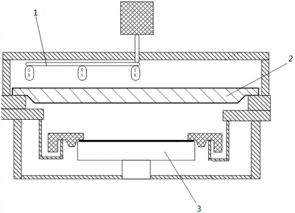
[0038] This embodiment provides a magnetron sputtering chamber for filling through-silicon vias, including: a chamber, a target disposed on the top of the chamber, a magnetron disposed above the target, and a magnetron disposed on the chamber. The base inside and under the target, the projected area of ​​the magnetron on the target is less than one-fifth of the target area, so as to increase the ionization rate of the medium gas, thereby increasing the filling rate of the through-silicon holes.

[0039] In the prior art, the projected area of ​​the magnetron on the target is generally 1 / 2 of the area of ​​the target, while the projected area of ​​the magnetron on the target used in the magnetron sputtering chamber provided by the present invention is less than One-fifth of the target area. Under the same power condition, the ionization rate of the medium gas will increase, thereby increasing the filling rate of the TSV.

[0040] Wherein, the projected area of ​​the magnetron ...

Embodiment 2

[0042] Other settings in this embodiment are the same as those in Embodiment 1, and will not be repeated here. The difference is that a magnetron includes magnetically opposite outer poles and inner poles surrounded by outer poles.

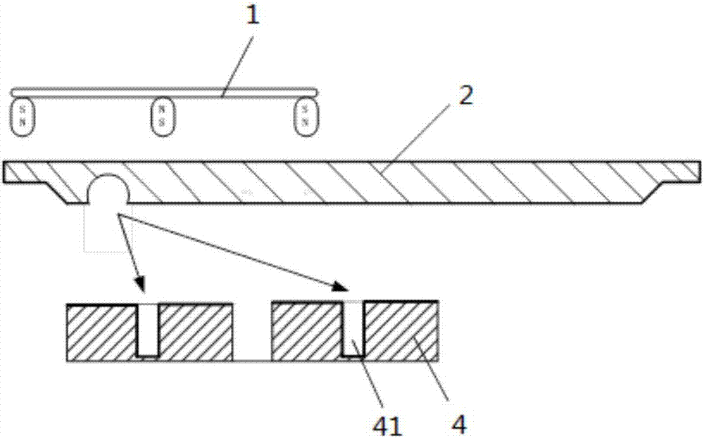
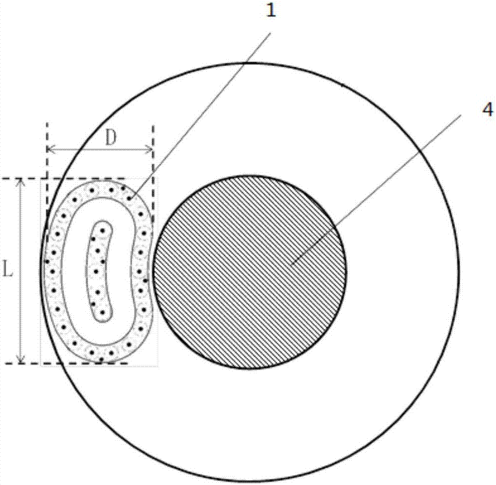
[0043] The magnetron in the magnetron sputtering chamber of the present invention includes magnetically opposite outer magnetic poles and inner magnetic poles, and the inner magnetic poles are surrounded by outer magnetic poles, further preferably as image 3 The kidney-type magnetron 1 is shown, and the magnetron can better ionize the medium gas. In addition, the outer magnetic pole of the magnetron 1 can be circular, rectangular or elliptical. Wherein, the outer magnetic pole has a long diameter L and a short diameter D, and the short diameter D is preferably less than or equal to 1 / 2 of the difference between the inner diameter of the chamber and the diameter of the wafer 4, that is, the short diameter D is less than or equal to the radius of ...

Embodiment 3

[0046] Other settings in this embodiment are the same as those in Embodiment 2, and will not be repeated here.

[0047] Its difference is that the magnetron sputtering chamber of this embodiment also includes a rotating mechanism, such as Figure 4As shown, the rotating mechanism 5 includes a rotating shaft 51, a first rotating arm 52 and a second rotating arm 53; one end of the first rotating arm 52 is fixedly connected to the rotating shaft 51, and the other end is connected to one end of the second rotating arm 53. The other end of the two rotating arms 53 is fixedly connected with the magnetron 1; there is an included angle between the first rotating arm 52 and the second rotating arm 53; the rotating shaft 51 drives the first rotating arm 52 and the second rotating arm 53 to rotate, thereby Drive the magnetron 1 to rotate.

[0048] Wherein, the connection mode between the first rotating arm 52 and the second rotating arm 53 can be a fixed connection or a flexible connect...


PUM


Abstract

The invention discloses a magnetron sputtering cavity and a semiconductor processing device for silicon through hole filling. The magnetron sputtering cavity comprises a cavity, a target material arranged on the top of the cavity, a magnetron arranged above the target material and a base which is arranged inside the cavity and under the target material; a projection area of the magnetron on the target material is smaller than one fifth of the area of the target material in order to improve an ionization rate of a medium gas so as to improve a filling rate for the silicon through hole. The semiconductor processing device comprises the magnetron sputtering cavity. The magnetron sputtering cavity and the semiconductor processing device improve filling efficiency of the silicon through hole.

Description

technical field [0001] The invention belongs to the field of semiconductor equipment, and in particular relates to a magnetron sputtering chamber for filling through-silicon holes and semiconductor processing equipment. Background technique [0002] Physical Vapor Deposition (PVD) is a widely used method for depositing metal layers and related materials during the fabrication of integrated circuits. At present, Through Silicon Via (TSV) technology is more and more widely used, which greatly reduces the interconnection delay between chips, and is a key technology for the realization of three-dimensional integration. The application of PVD in TSV is mainly to deposit a barrier layer and a copper seed layer inside the TSV. The function of the barrier layer is to prevent the diffusion of copper into silicon or silicon dioxide, and the function of the copper seed layer is to prepare for the subsequent electroplating process. A conductive layer, so the deposition of barrier and c...

Claims


Application Information

Patent Timeline
Patent Type & Authority Applications(China)
IPC IPC(8): H01L21/67C23C14/16C23C14/35
CPCC23C14/165C23C14/35H01L21/67011
Inventor 侯珏王厚工丁培军
Owner BEIJING NAURA MICROELECTRONICS EQUIP CO LTD
Why Eureka
Try Eureka