Gallium oxide single crystal based radiation detector and preparation method thereof

A radiation detector, gallium oxide technology, applied in the direction of semiconductor devices, electrical components, circuits, etc., can solve the problems of small signal, lack of device manufacturing technology, no radiation detectors, etc., to achieve simple process manufacturing technology, solution The effect of preparing puzzles

Active Publication Date: 2017-08-18
DALIAN UNIV OF TECH
View PDF3 Cites 9 Cited by
  • Summary
  • Abstract
  • Description
  • Claims
  • Application Information

AI Technical Summary

Problems solved by technology

However, there have been no reports on the preparation of radiation detectors based on gallium oxide single crystals
The main reasons are: 1. High-quality gallium oxide single crystal has only been successfully developed recently. 2. The particles or rays emitted by the radiation source have extremely high penetrating ability, and the energy deposition rate in the semiconductor is low, so th

Method used


Image

  • Gallium oxide single crystal based radiation detector and preparation method thereof
  • Gallium oxide single crystal based radiation detector and preparation method thereof
  • Gallium oxide single crystal based radiation detector and preparation method thereof

Examples


Embodiment 1

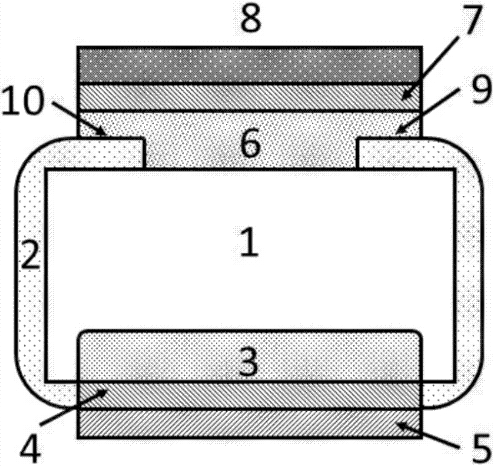
[0053] This embodiment provides a radiation detector based on gallium oxide single crystal, including the following process steps:

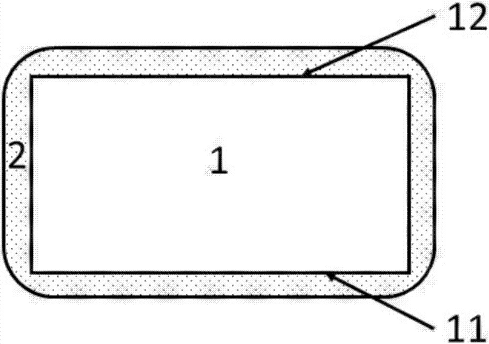
[0054] Step 1: Select a high-resistance gallium oxide single crystal with a thickness of 300 μm and a surface of 5 mm square, and pre-deposit SiO with a thickness of 2 μm on its upper surface and sides 2 The protective layer;

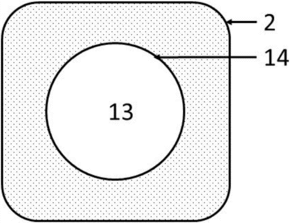
[0055] Step 2: making a circular opening with a diameter of 4 mm in the center of the lower surface of the gallium oxide single crystal;

[0056]Step 3: on the lower surface described in step 2, pre-deposit a layer of 100nm thick tin layer by thermal evaporation;

[0057] Step 4: Seal the above-mentioned gallium oxide single crystal in a quartz tube, and the vacuum degree in the quartz tube is 3×10 -4 Pa;

[0058] Step 5: Put the quartz tube sealed with gallium oxide single crystal into a tube furnace for heat treatment at a temperature of 1000°C for 12 hours;

[0059] Step 6: After the temperature drops to room temper...


PUM

PropertyMeasurementUnit
Thicknessaaaaaaaaaa
Thicknessaaaaaaaaaa
Thicknessaaaaaaaaaa

Abstract

The invention belongs to the technical field of semiconductor device preparation, and relates to a gallium oxide single crystal based radiation detector and a preparation method thereof. The radiation detector takes a high-resistance gallium oxide single crystal as a substrate, the upper and lower surfaces and the side surfaces of the gallium oxide single crystal are provided with an SiO2 protection layer, a tin-doped gallium oxide layer, a titanium layer and a gold layer which are formed by tin atom diffusion are sequentially arranged in a mask pattern formed at the lower surface of the SiO2 layer of the gallium oxide single crystal; and a nickel layer, a titanium layer and a gold layer are sequentially arranged in a mask pattern formed at the upper surface of the SiO2 protection layer of the gallium oxide single crystal, and each layer has an overlapping region with the SiO2 protection layer retained at the upper surface. The invention provides an effective, simple and convenient processing and manufacturing technology, a problem of preparation for a high-performance gallium oxide radiation detector is solved, and the development of a novel gallium oxide based radiation detector is realized.

Description

technical field [0001] The invention belongs to the technical field of semiconductor device preparation, and relates to a radiation detector based on a gallium oxide single crystal material and a preparation method thereof. Background technique [0002] The third-generation wide-bandgap semiconductor materials represented by gallium oxide are widely used in high-frequency, high-power, It has important applications in electronic devices such as radiation resistance. In particular, gallium oxide has a band gap as high as 4.9eV and a breakdown electric field of 3.5×10 6 V / cm, ionization energy of 5.9eV, non-doped epitaxial film resistivity greater than 10 7 Ω·cm, the average atomic number is 17.2, the melting point is 1740°C, and the Ga-O bond energy reaches 363.6KJ / mol. It is an ideal material for the development of semiconductor radiation detectors. People have mastered several methods for preparing gallium oxide single crystals and gallium oxide films. The directly prepar...

Claims


Application Information

Patent Timeline
IPC IPC(8): H01L31/115H01L31/032H01L31/18
CPCH01L31/032H01L31/115H01L31/18
Inventor 夏晓川梁红伟
Owner DALIAN UNIV OF TECH
Why Eureka
Try Eureka