

Active switch array substrate and manufacturing method thereof and display panel
A manufacturing method and switch array technology, applied in the field of display screens, can solve the problems of huge investment in equipment, complex processes, and high production costs, and achieve the effects of reducing production costs, improving efficiency and production capacity, and shortening production time
- Summary
- Abstract
- Description
- Claims
- Application Information
AI Technical Summary
Problems solved by technology
Method used
Image

Examples
Embodiment Construction
[0055] In order to make the technical problems, technical solutions and beneficial effects to be solved by the present invention clearer, the present invention will be further described in detail below in conjunction with the accompanying drawings and embodiments. It should be understood that the specific embodiments described here are only used to explain the present invention, not to limit the present invention.
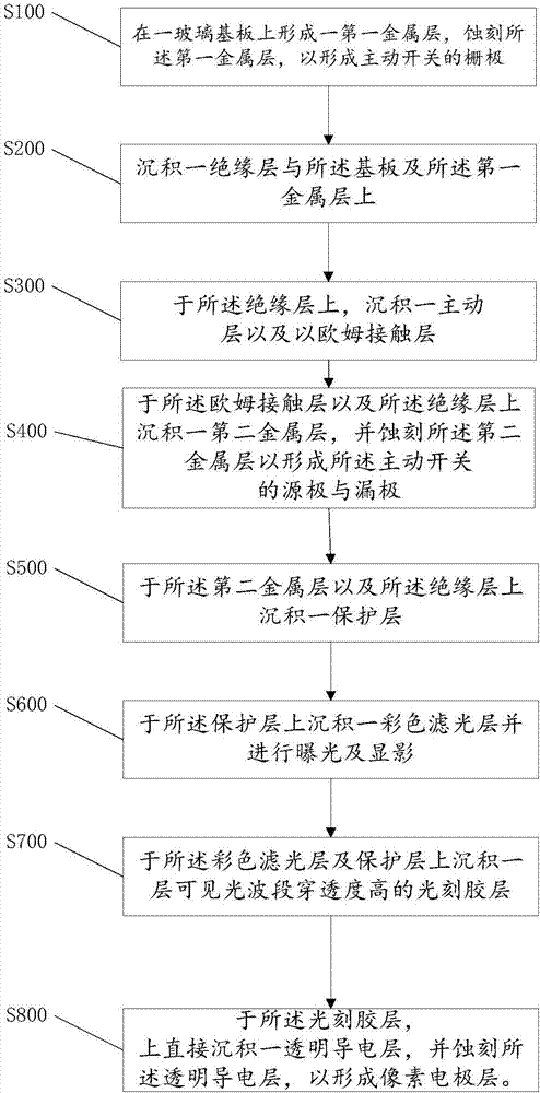
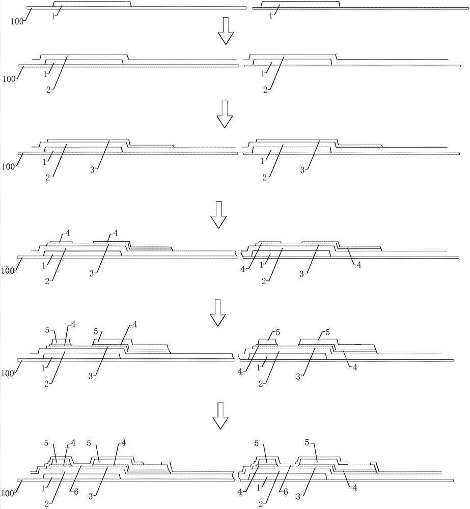
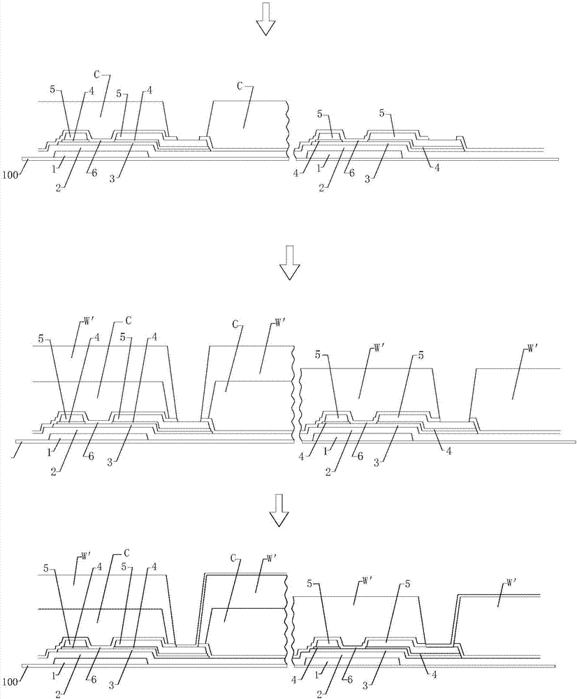
[0056] Such as figure 1 and figure 2 As shown, an embodiment of the present invention provides a method for manufacturing an active switch array substrate, including the following steps:
[0057]Step S100, forming a first metal layer on a substrate 100, and etching the first metal layer to form the gate 1 of the active switch;
[0058] Step S200, depositing an insulating layer 2 on the substrate 100 and the gate 1;
[0059] Step S300, depositing an active layer 3 and an ohmic contact layer 4 on the insulating layer 2;
[0060] Step S400, depositing a second me...
PUM
 Abstract
Description
Claims
Application Information